Physicists in the US have made the first ultrathin flat lens. Thanks to its flatness, the device eliminates optical aberrations that occur in conventional lenses with spherical surfaces. As a result, the focusing power of the lens also approaches the ultimate physical limit set by the laws of diffraction.
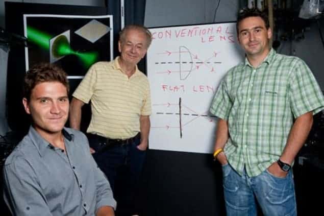
“Imagine if you were to replace the lens in a mobile phone with a flat and ultrathin one – you could then squeeze your smartphone down to a thickness approaching that of a credit card,” says team leader Federico Capasso of the Harvard School of Engineering and Applications. “Most optical components found in devices today are quite bulky because the light-beam shaping is done by changing the optical path of incident light rays, which requires changes in lens thickness. In our lens, all the beam shaping is done on its flat surface, which is just 60 nm thick.”
In an ordinary lens, light rays travel more slowly in the thicker, central regions than in the thinner, peripheral ones thanks to the smaller phase velocity of light in glass compared with air, he explains. This distribution of phase delays in the lens leads to light refraction and focusing.
Nanostructured metasurface
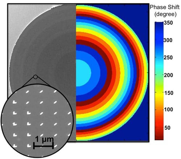
The new flat ultrathin lens is different in that it is a nanostructured “metasurface” made of optically thin beam-shaping elements called optical antennas, which are separated by distances shorter than the wavelength of the light they are designed to focus. These antennas are wavelength-scale metallic elements that introduce a slight phase delay in a light ray that scatters off them. The metasurface can be tuned for specific wavelengths of light by simply changing the size, angle and spacing between the nanoantennas.
“The antenna is nothing more than a resonator that stores light and then releases it after a short time delay,” Capasso says. “This delay changes the direction of the light in the same way that a thick glass lens would.”
The lens surface is patterned with antennas of different shapes and sizes that are oriented in different directions. This causes the phase delays to be radially distributed around the lens so that light rays are increasingly refracted further away from the centre, something that has the effect of focusing the incident light to a precise point.
No monochromatic aberrations
The new lens does not suffer from the image-distorting features, known as monochromatic aberrations, that are typical of lenses with spherical surfaces, adds Capasso. “Spherical aberration, coma and stigmatism are all eliminated and one gets a well-defined diffraction-limited, accurate focal spot. This is true even when light rays hit the lens away from the centre or at a large angle, so no complex corrective techniques are required.”
The Harvard team made its lens by first depositing a nanometre-thin layer of gold. The researchers then stripped away parts of the gold to leave behind an array of V-shaped structures (the nanoantennas) that were evenly spaced in rows across the surface of a silicon wafer.
The most obvious applications for the lens include photography and microscopy, says Capasso. “For example, compact objectives with very large numerical apertures can be envisaged, but we can also imagine optical fibres with patterned facets for new imaging and medical applications, and anywhere in general where a conventional lens could be replaced with a flat one,” he says.
Towards broadband focusing
Although the lens is only at the proof-of-concept stage, Capasso and colleagues have already been inundated with requests from photographers and astronomers from around the world. The focusing efficiency of the lens is still quite small at present but, according to the team, could easily be increased by increasing the packing density of the optical antenna and by using different flat-lens designs. “So far, the lens only focuses specific wavelengths of light but by arranging different antenna patterns onto the metasurface it could be made broadband,” says Capasso.
The researchers fabricated their lens using electron-beam lithography, which is not the most practical technique because it is time-consuming. “Fortunately, there are many emerging nanolithography technologies that could be suitable for mass production, such as nanoimprinting and soft lithography, which might be extremely useful for patterning our lens on flexible substrates,” adds Capasso. “This in itself would open up a host of exciting application areas.”
The results are reported in Nano Letters.


