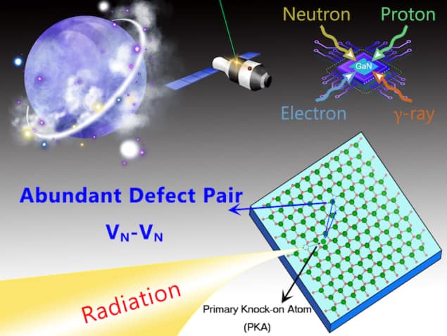
Gallium nitride (GaN) is the world’s second-favourite semiconductor, present in devices ranging from light-emitting diodes and photodetectors to high-temperature electron mobility transistors. When these devices are exposed to irradiation from high-energy particles – as they often are in fields such as satellite communications, aerospace, defence and the nuclear industry – they are prone to developing defects that degrade their electronic properties.
Researchers at East China Normal University in Shanghai and Shanxi University in Taiyuan have now performed the first systematic study of a class of GaN defects known as defect pairs. Such structures have been little studied to date, and the researchers say that understanding them and the mechanisms that cause them may help boost the radiation resistivity of GaN-based devices.
For equipment in low-Earth orbit, the most common forms of damaging radiation are proton, electron and gamma radiation. In a nuclear-industry context, the chief culprit is usually radiation from neutrons. These high-energy particles can create a dizzying array of defects in GaN, including point defects, defect pairs and complexes, and disordered regions in the material’s semiconductor lattice. The point-defect “family” alone contains six sub-types of defect, known as VGa and VN vacancies, GaN and NGa anti-sites and Gai and Ni interstitials.
21 different types of defect pairs
The properties of these point defects have been well-studied over the last three decades. However, defects of this type can also bind with each other to form less-common defects, including double-site defect pairs and multiple-site defect complexes. In principle, 21 different types of defect pairs can form, each with its own structural configuration.
Fortunately for GaN device designers, these exotic defect pairs usually require much higher energy to form than single-point defects. Freshly-synthesized GaN typically contains them only in low concentrations, and for this reason only a handful of defect pairs, such as VGa-VN and VGa-GaN, have been studied in any detail.
In radiation-damaged samples, however, the concentration of the high-energy defect pairs can be much greater. This led Shiyou Chen and his colleagues to study all 21 defect pairs in GaN, performing first-principles calculations of their structures, formation energies and transition energy levels.
Their results show that after a high-energy particle strikes the GaN and triggers a defect-inducing “collision cascade”, the defect pairs that form are generally stable. Such pairs are separated by short distances and nine of them have formation energies lower than 10 eV. In terms of their effect on the material’s properties, they mostly act as electron donors, producing many defect levels in the band gap of GaN and potentially impairing the performance of GaN-based devices.
Fundamental parameters for future multiscale simulations
Among the different defect pairs, the researchers found that the VN-VN vacancy pair has an especially low formation energy and can therefore be produced in high concentrations in p-type and Ga-rich GaN. This fact was overlooked in previous work, Chen says.
Hydrophobic or hydrophilic? Aero-gallium nitride is both
“The defect formation energies and transition energy levels we have calculated will be fundamental parameters for future multiscale simulations of radiation damage processes in GaN,” he tells Physics World. “These models may help us find efficient methods to improve the radiation resistivity of GaN and increase the lifetime of devices made from this semiconductor.”
In the present work, which is detailed in the Journal of Semiconductors, the researchers only looked at defect pairs formed by intrinsic defects. They say they will now be investigating pairs and clusters formed by intrinsic dopants (such as Mg, C, H and O) and defects. These defect-dopant structures naturally form in GaN samples grown using techniques such as metal-organic chemical vapour deposition (MOCVD) and hydride vapour phase epitaxy (HVPE).


