Scientists in the Republic of Ireland, the US and the UK have discovered that nanocrystalline copper films are not as flat as they may seem. Using scanning tunnelling microscopy (STM) to map the surfaces of copper films with atomic detail, the researchers revealed that the grains in copper rotate and misalign in an effort to reduce grain boundary energy, resulting in a surface topography marred by valleys and ridges. The roughness of this surface is predicted to have a pronounced effect on the role of nanocrystalline metals in integrated circuits.
Nanocrystalline metals comprise nanoscale grains containing upward of a million atoms arranged in a well ordered crystalline structure. Microchip technology relies on the use of nanocrystalline metals and patterned films as electrical contacts and interconnect components in integrated circuitry. The utility of these materials depends largely on their thermal and electrical conductivities, properties which are greatly affected by how the grains fit together. Structural defects, misalignments and dislocations lead to surface roughening of nanocrystalline metal films, inducing processes that affect electronic transport and hamper their performance.
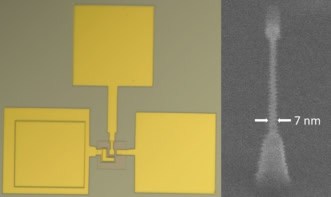
For copper, in which grains tend to grow with one specific surface orientation, it would be expected that the grains and grain boundaries form a continuous, flat surface. However, this does not seem to be the case. Xiaopu Zhang and John Boland, at Trinity College Dublin, and co-workers at University of Pennsylvania, Intel Corporation, and Imperial College London, used STM to generate a topographic map of the surface of a thin copper film. The researchers discovered valleys and ridges a few nanometres in depth and height where grain boundaries emerge at the surface.
Zhang and colleagues corroborated their analysis of the topographical data with simulations to show that these valley and ridge features arise from low-angle rotation of the grains. Grain boundary energy is minimized in a complex way by maximizing the distance between structural defects. Furthermore, valleys and ridges can be treated as complementary features, as simulations reveal that a grain boundary which forms a valley at the top surface of a copper film also forms a ridge at the bottom surface, and vice versa.
These findings suggest that perfectly flat surfaces are impossible, not only for copper but also for other structurally similar metals such as gold and silver, whose utility is hugely dependent on surface smoothness. The results allow a new perspective on the engineering of such materials for technical applications that is vital for the advancement of high-performing electronics. With this knowledge, the researchers suggest it may be possible to tailor the processing conditions of nanocrystalline metals – by techniques such as grain boundary doping, and controlling the interface between the film and substrate – in order to finely tune their properties for precise functionality.
Full details are reported in Science.