Ultra-precise electron beams can rearrange atoms in a 3D crystal lattice and create structures not found in nature, an international team of researchers has shown. The work could have implications for quantum simulation and atomic-scale manufacturing.
The 1986 Nobel Prize for Physics was divided between three researchers. Half was split between Gerd Binnig and Heinrich Rohrer of IBM’s Zurich laboratory for their development of the scanning tunnelling microscope (STM). The STM’s ability not just to image but to move atoms was famously demonstrated three years later, when Don Eigler and Erhard Schweizer of IBM Almaden in California produced a picture of 35 xenon atoms precisely placed on a crystal of nickel to spell out the letters “IBM”. STMs have become widely used in surface analysis. However, they can only manipulate 2D surfaces, are painstakingly slow and require high vacuum and ultracold temperatures.
The other half of the 1986 prize went to Ernst Ruska of Germany’s Max Planck Society for his invention of the electron microscope – which can image samples with atomic resolution. Until now, however, electron microscopes had not been able to deterministically manipulate atoms because their high-energy electron beams tend to break bonds randomly within a crystal.
Now researchers in the group of Frances Ross at Massachusetts Institute of Technology led by Julian Klein, together with Kevin Roccapriore of Oak Ridge National Laboratory and others, used Oak Ridge’s ultra-precise, extremely stable, focused electron beam to penetrate around 13 nm into a crystal of the layered van der Waals material chromium sulphide bromide.
Interesting crystal structure
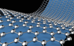
“The material has a very interesting crystal structure,” says Klein; “One individual layer has a mixture of sulphur and chromium atoms, but then on both sides of this layer there are bromine atoms sticking out in both directions. And when you stack those crystals you create atom-sized gaps between the layers.”
When the electron beam is positioned within 20 pm of its target and then moved slightly in a specific direction, the electrons in the beam can nudge the chromium atoms in the line of fire out of their original positions into the target unoccupied sites. This creates lattice defects called vacancy–interstitial complexes. Computer simulations suggest that, owing to interlayer interactions, movement of the chromium atom in one layer should encourage the transformation of layers above or below. Ross says that “[the transformed layers] do form in a timed sequence, but we can’t tell in what order they’re transforming”.
By carefully manipulating the electron beam across the surface of the crystal, the researchers can create an array of vacancy–interstitial complexes: “Julian and Kevin have a series of images at different times,” says Ross; “You can see the quality of the result just gets better and better…The beam has to be exactly on that column of atoms because otherwise some of the energy is going to go into the wrong place and disrupt the rest of the lattice.”
More robust crystals
The resulting 3D crystal is much more robust than an STM-created surface. “The defects created in the interior of the crystal are protected from the environment,” Ross explains. This allows measurements of different properties in different laboratories without needing cryogenic refrigeration or vacuum.
‘Nano-aquariums’ deliver atomic-resolution imaging
This could also ease the path to practical application for what is, say the researchers, an emergent many-body state. “That’s where the fun stuff comes in,” Ross says. “I’m excited because of the scalability of this that allows us to look at the interactions between the defects rather than just creating a defect itself. The stability of the microscopes that allows us to keep going and create a huge array is really exciting.” The researchers are examining various possible applications in, for example, quantum simulation and the manufacturing of matter with atomic-scale precision.
The team describes its work in Nature.
“It’s a fascinating paper,” says materials scientist and STM expert Ludwig Bartels of the University of California, Riverside. “It’s definitely above the scale of what scanning tunnelling microscopy could do…and, as they discussed in their paper, it’s probably a really interesting scale in which they can think about electronic states extending between the different defects they are making.”
He says that, while he does not believe this will ever be the way computer chips are made “it is definitely an order of magnitude above what was possible before”. Moreover, he says that the ideas used in the paper to monitor the motion of the atoms remind him of those developed 30 years ago for STM. “They are not exactly the same, but they are reminiscent, and they are just as ingenious,” he says.