Graphene plasmonics has been caught between a rock and a hard place, with high-energy plasmons readily coupling into hybrid modes, while low-energy plasmons are prone to damping. Now researchers in Japan, Germany and Singapore report in the first issue of Journal of Physics: Materials how they can protect low-energy plasmons from damping by encapsulating the graphene in hexagonal boron nitride (hBN). What is more, in the same issue another group of researchers demonstrate a transfer-free process that could enable mass-production of high-quality hBN-encapsulated graphene devices.
Not high energy proves no great loss
Plasmons – the collective excitations that couple the electromagnetic fields associated with incident light to the electrons in a material – have long attracted interest for potential applications including high-sensitivity sensing and information processing. Graphene plasmons hold the additional allure of being tunable, but so far it has been difficult to produce graphene plasmons that remain uncoupled to surface modes, which form hybrid plasmon-polaritons, while avoiding ohmic losses.
“Tunability is always interesting because then you can really have a recipe, which tells you not just how to generate a property, but also how to switch it on and off,” says ICREA research professor Stephan Roche, editor-in-chief of Journal of Physics: Materials in his discussion of some of the papers in the first issue.
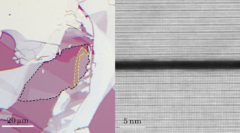
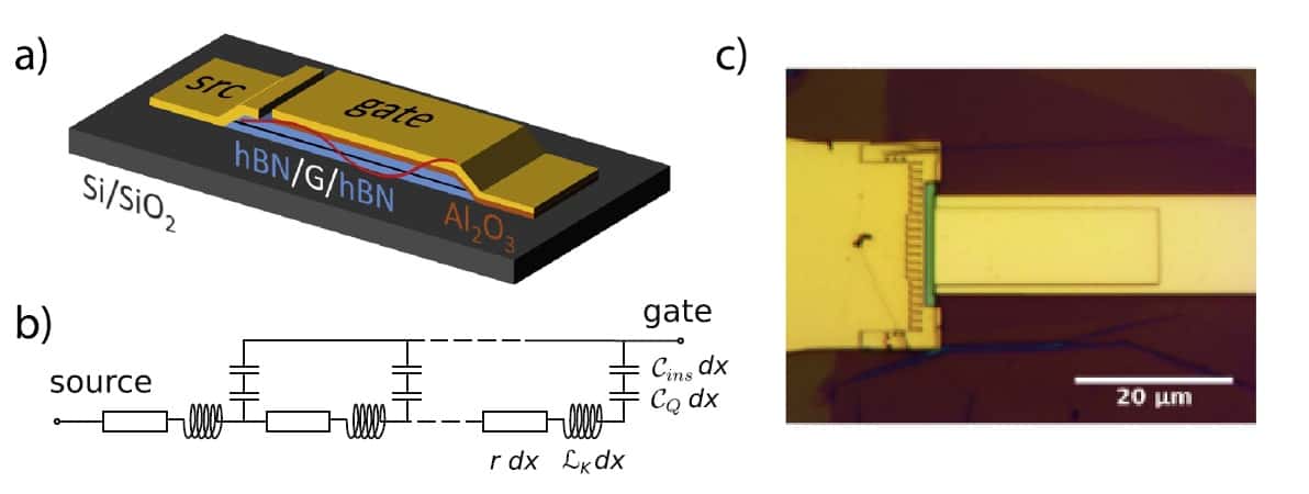
By encapsulating high-quality exfoliated graphene in hBN Bernard Plaçais at Sorbonne University in France and his collaborators produce devices where the graphene plasmons are both very weakly coupled to any other source and have a high Q factor. They demonstrate the approach in plasma resonance capacitors with a 100 μm quarter-wave plasmon mode, at 40 GHz, and a quality factor of around two.
“Our capacitor GHz experiment constitutes a first step toward the demonstration of plasma resonance transistors for microwave detection in the sub-THz domain for wireless communications and sensing,” they point out in their report. “It also paves the way to the realization of doping modulated superlattices where plasmon propagation is controlled by Klein tunnelling.”
Producing better quality and bigger quantities
In the same issue Vincent Bouchiat and colleagues at the University of Grenoble and CNRS in France, and the National Institute of Material Science in Japan report how to produce hBN encapsulated graphene with fewer defects by chemical vapour deposition, a technique that readily lends itself to upscaling production.
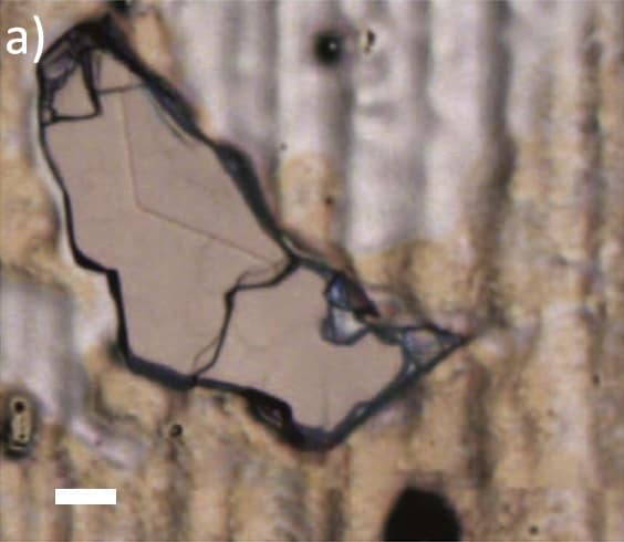
As with the work by Plaçais and colleagues, when researchers want to show how to exploit graphene’s unique optoelectronic properties in a given device, the preferred graphene fabrication technique is exfoliation, where individual layers are stripped of pristine graphite. However – production scale limitations aside – transferring exfoliated layers of graphene onto hBN inevitably introduces defects, which impinge on the device performance. Instead by growing the boron nitride and then the graphene together without changing the growth parameters Bouchiat and his team show that they can produce high-quality large-area encapsulated graphene with a charge carrier mobility that reaches 2.0 × 104 cm2V-1s-1.
“These two papers are very illustrative of the challenges of research in 2D materials,” says Roche, who was not involved in either piece of research. “On one side you have the forefront of research trying to get really high-quality research devices, and then trying to explore what is unique about these 2D materials, and to demonstrate that they can really bring high value in terms of applications. Then on the other side you have people making efforts to integrate these materials and to upscale their growth so that they can be practical for industries in the medium term.”
A new player hits the scene in materials science

Whether the potential of the reported CVD approach can provide mass production of the graphene plasmonic devices remains to be seen. Full details of both reports are found in Journal of Physics: Materials issue 1.