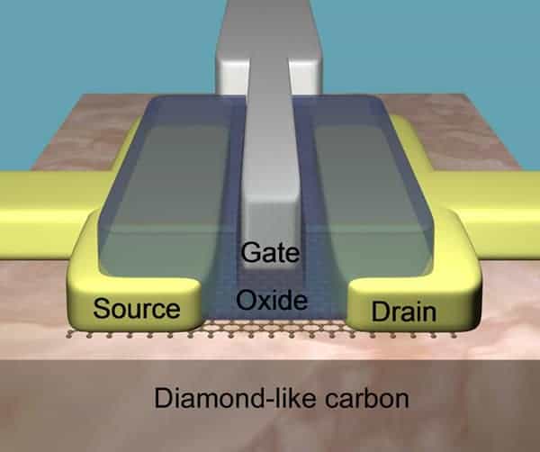
Diamond-like carbon could be an ideal substrate for graphene transistors. So say researchers in the US who have made advanced devices with a record-high cut-off frequency of 155 GHz and the shortest gate length ever of just 40 nm. The field-effect transistors, which also function all of the way down to temperatures as low as 4.3 K, operate at radio frequencies and so could be used in wireless communications.
Graphene is a flat sheet of carbon just one atom thick that conducts electrons at extremely high speeds. Indeed, the electrons behave like relativistic particles with no rest mass. This, and other unusual physical properties, means that graphene is often touted to replace silicon as the electronic material of choice and might be used to make faster transistors than any that exist today.
Transistors made from graphene could be used in radio-frequency microelectronic devices for wireless communications. These devices can be made by transferring high-quality graphene sheets, produced by a technique called chemical vapour deposition (CVD), onto a suitable, insulating substrate – such as silicon dioxide. However, the problem is that the substrate can severely degrade the electronic properties of graphene because of scattering of charge carriers (electrons and holes) in graphene. This scattering, which drastically limits the speed of the electrons and holes, comes about due to interactions between graphene and the dielectric substrate material.
Diamond-like, but cheap
Now, Phaedon Avouris and colleagues at the IBM Thomas J. Watson Research Center, New York, may now have come up with an answer to this challenge. The team used diamond-like carbon as the top layer of the substrate, with the carbon atop a standard silicon wafer. Diamond-like carbon is already widely used in the semiconductor industry and is created by chemical vapour deposition (CVD). It is a non-polar dielectric material, which means that it does not trap charges nor does it scatter charge as much as silicon dioxide does. It is also cheap to make in large areas; does not absorb much water; and has excellent thermal conductivity.
“The cut-off frequency we obtained is the highest so far for transistors made from CVD-graphene,” Avouris said. “However, it is not, by far, the limit of what can be achieved because the quality of the CVD-graphene we used was modest (it’s carrier mobility was less than 1000 cm2/Vs).”
At IBM and many other laboratories around the world, scientists are now perfecting the CVD process and steadily increasing its performance, he added.
High-frequency transistors could find use in a wide range of applications, but primarily in communications – for example, mobile phones, the Internet and radar. Medical imaging, security and sensors could also benefit. What’s more, the new transistors continue to work well at extremely low temperatures and could therefore be used in extremely cold environments, such as space.
“With this work, another industry compatible technology option for radio-frequency graphene field-effect transistors is now available,” commented Frank Schwierz of the Ilmenau Technical University in Germany.
The results are published in Nature 472 74.


