Graphene could be the two-dimensional nanomaterial for the future, but exploiting it will require further advances in methods to fabricate it. With a high carrier mobility, stability, and rigidity under atmospheric conditions, its electronic, chemical, and structural properties are unparalleled. In particular, AB stacked bilayer graphene, which consists of two graphene sheets stacked in an offset configuration, has an impressive tuneable bandgap ideal for usage in high performance device fabrication. However, growth of defect-free graphene and large-scale transfer from its native growth substrate, a necessity to bring such applications to fruition, remains challenging. Researchers Hussain Alsalman et al., under the direction of Michael Spencer, hope to overcome these challenges with their novel growth and dry transfer method.
High-quality graphene growth
Large-scale, uniform, defect-free graphene samples are difficult to obtain. Traditional exfoliation methods, where flakes of graphene are mechanically scraped off of graphite, are limited to small areas. Chemical vapour deposition (CVD) performs slightly better regarding area but it can take hours to achieve AB stacked sheets.
To overcome these obstacles, researchers at Cornell University utilized SiC epitaxy to grow large areas of graphene up to hundreds of microns,. Essentially, they annealed a prepared layer of SiC and the Si atoms sublimated to leave a layer of carbon that rearranged into graphene. Hussain Alsalman, a graduate student working on the project, notes, “SiC epitaxy sublimates the silicon atoms across the entire SiC wafer surface at once, giving it a clear advantage in the speed of single crystal synthesis.”
They then obtain bilayer graphene through high-temperature hydrogen intercalation. As Alsalman et al. point out in their report of the work, “SiC graphene on the Si-face is not limited by the orientations randomness that challenges CVD graphene.” This control over the AB stacking is another clear advantage over traditional synthesis methods.
A novel transfer method
Since SiC epitaxy produces graphene on an undesirable SiC substrate, the next step is isolating it from its native growth substrate, and this is not trivial. Alsalman et al. resolved this issue by transferring the graphene layers to more functional materials.
First, they deposited a layer of gold onto the graphene/SiC stack and spin-coated the stack to deposit a layer of acrylic polymer on top of the new gold layer. They can then mechanically remove the original SiC substrate thus allowing transfer of the graphene to the new target substrate. The acrylic and gold layers they remove via acetone and etching, respectively. Lastly, they rinse the isolated graphene/substrate stack to obtain the final product.
So many materials
Read more

So many materials
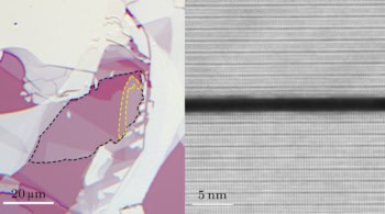
Structural and electronic characterization
To emphasize the success of their dry transfer method, Alsalman et al. employed a range of characterization techniques. Transmission electron microscopy (TEM) data show the classic atomic honeycomb structure of graphene and reveal high crystallinity within the monolayers even after transfer, which the researchers describe as “a testament to the robustness of epitaxial graphene.”
Although Raman spectroscopy revealed few defects within the graphene structure and uniform AB stacked bilayers, these results were not as impressive as those from monolayer growth via SiC epitaxy, most likely due to the intercalation method used to generate the second graphene layer. In their report of the work Alsalman et al. state, “This limitation for bilayers might be mitigated by carefully selecting for growth of bilayer on SiC and not using intercalation…However, this process needs optimization and would be a topic of further research.”
Field effect transistors (FETs) constructed from graphene grown with this technique also highlighted discrepancies in the quality between monolayer and bilayer graphene. While monolayer FETs showed field effect mobilities of approximately 1700 cm2/Vs, bilayer devices lagged behind this value at 250 cm2/Vs. Annealing the graphene before device construction increased the mobility values, which the researchers attribute to release of trapped hydrogen gases. The increase was limited to around 25%, and these generally low mobility values may be due to defects caused by step edges present on the SiC wafers. Control of bilayer growth, as previously discussed, may also increase the mobilities.
TLM devices gave contact resistance values of approximately 585 Ω μm for monolayer samples and 2310 Ω μm for AB stacked samples. Such a result is unsurprising, as contact resistance directly depends on the quality of the graphene, which was worse for the bilayer samples compared with the monolayer samples. Carrier mobilities also affect resistance.
Limitations aside the researchers conclude, “And while the performance figures might fall short from that of CVD graphene, transferred epitaxial graphene does currently have an advantage in synthesizing large area AB stacked bilayer graphene where in principle it is only limited by the size of the SiC wafer.”
Full details are reported in Nano Futures.