While not the first to be plagued by fine webbing effects spoiling their laser-written structures, Joel K W Yang’s group have been the first to exploit it to achieve feature sizes below 10 nm. “A lot of interesting physical phenomena such as quantum confinement and plasmonic field enhancements occur at these length scales,” Yang points out.
Yang, an associate professor at the Singapore University of Technology and Design (SUTD), had been focusing his research on high-resolution nanofabrication methods and their applications. Having worked with electron-beam lithography, where he was routinely able to achieve sub-10 nm feature sizes, he turned his attention to direct laser writing (DLW), keen to see how far he could push the resolution he could achieve with this technology.
DLW has the advantages of speed and simplicity over ion- and electron-beam lithography, which require vacuum technology and are slow and fiddly to implement. However, DLW is traditionally limited to feature sizes of hundreds of nanometres, around 10 times bigger than ion- and electron-beam lithography. Smaller feature sizes are possible by modifying the equipment and incorporating stimulated emission depletion lithography, but Yang was interested in pushing the basic method to its limits. So when his student complained about webbing structures that he could not get rid of, Yang suggested, “What if instead of getting rid of them we investigate how to control them.”
Intensity matters
DLW exploits two-photon absorption to create cross-linking molecules from a resin, which then link up where the laser beam “writes” the structure. The remaining resin is then washed away. Yang and his co-workers used a 780 nm wavelength laser. As the resin absorbs light with a wavelength below 400 nm, it will only absorb light at the focus of the beam where the light intensity allows absorption of two lower-energy 780 nm photons.
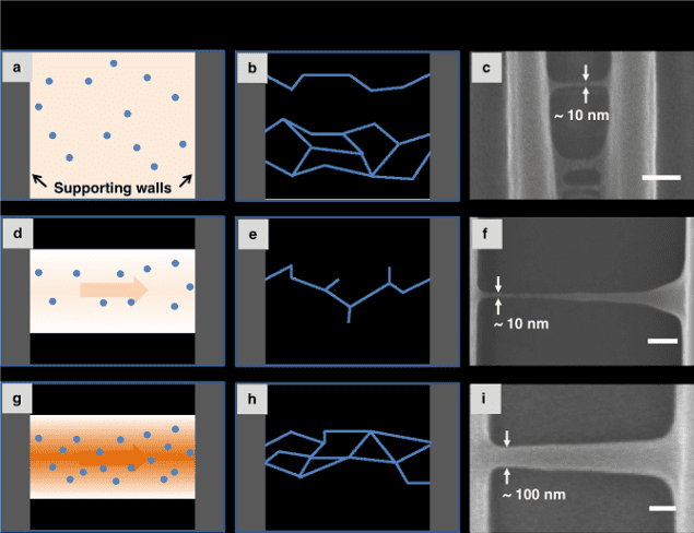
The problem is that fine filaments still form outside where the laser focus has written. “Above-threshold laser powers can cross-link polymers in the wake of the beam but lower powers lead to lower concentrations of crossilinking molecules in the wake,” says Yang. “We think at low power you need a percolative pathway for cross-linking to happen, so you have regions where the concentration is just high enough.”
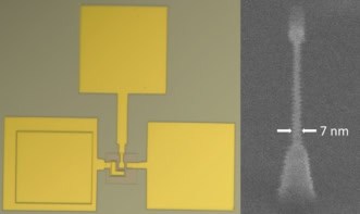
To exploit these effects Yang and colleagues used a laser at half power to control the spread of these filaments from the wall of one structure to another. This way they could write 20 nm features with a yield of 80% and with some filaments as narrow as 7 nm only 33 nm apart. The filaments grow with residual tensile strain that pulls the walls down if they are not well anchored to the substrate. However, Yang points out that this strain is actually helpful for making the filaments thinner.
“There’s a game where you pick up drinking straws – you stretch it to make it really thin, and use it to saw one another’s straws to see whose straw would break first. It’s a similar effect here,” says Yang.
Pushing DLW further
With improvements to the chemistry of the resin so that the cross-linked material has greater structural integrity to resist fragmenting, Yang thinks even smaller feature sizes should be possible. The team has already experimented with writing a series of filaments that are vertically displaced so that closer lateral spacing is possible without the features merging. It may also be possible to pattern filaments at off-normal angles to the anchoring structures, although Yang expects the angles may be limited to within 10° of the normal as that is the shortest percolation path.
Yang is still keen to better understand the mechanism of the sub-threshold intensity ultrafine DLW and improve the uniformity of the features. At present the filaments grow thicker towards the adjoining wall, most likely due to thermal effects.
Possible applications include use as a template resist for plasmonic structures and 4D printing, where the strain can act as an actuator for printing dynamic structures defined in space and time.
Full details are reported in Nano Futures, and for more research on sub 10 nm nanofabrication visit the Nanotechnology focus collection.


