While solar farms offer clean and reliable energy production, they are space-consuming and remain unfeasible for use in urban centres and outer space. An alternative solar solution for the near-future rests in micron-thin photovoltaics. These devices couple the low-cost manufacturing of silicon with the low weight and flexibility of thin films.
Led by Marian Florescu and Esther Alarcon-Llado, researchers from the University of Surrey, Imperial College London, and AMOLF’s Center for Nanophotonics partnered to address the shortfalls of existing thin film solar panels. Their newly released paper in ACS Photonics describes the properties of the photovoltaic device they devised and tested.
Absorbance through light trapping
The primary issue with increasingly thin solar cells is that with lower thickness comes lower light absorbance efficiency — a majority of light either reflects off the surface or passes through entirely. “Nearly a third of light bounces straight off [the material] without being absorbed and the energy harnessed,” says Florescu, adding, “a textured layer across the silicon slab helps tackle this problem.”
By texturing the surface of the silicon, incident sunlight is instead diffracted into the plane of the silicon thin film, “trapping” the light in the material. Regular ordered patterns are insufficient for this task, as they only diffract sunlight at specific wavelengths and angles of incidence. Alternatively, disordered patterns can scatter a broad range of wavelengths into the film but are not particularly efficient.
Instead, the team employed a specific surface design called hyperuniform disordered (HUD) patterns. HUD media have constrained randomness, which causes them to behave like ordered solids rather than amorphous materials. As such, they are particularly useful in engineering light scattering and diffraction.
The researchers etched HUD patterns into the top 200 nm of a 1-micron-thick silicon film (see above figure). Then they topped the film with a spin-coated polymer resist, which reduced its reflectance by making its index of refraction closer to that of air. Through this combination of techniques, the team recorded a solar absorbance of 66.5% – a staggering increase from the 25.5% absorbance of unadulterated films. This improvement resulted in an absorption equivalent photocurrent of 26.3 mA/cm2, which tops the next-best reported result of 19.72 mA/cm2 for a cell of similar thickness.
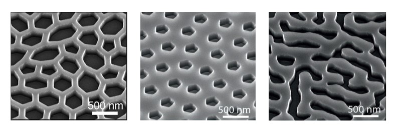
Which HUD pattern?
The team tested multiple HUD patterning designs, including a HUD network, HUD holes and a spinodal pattern (left to right, above image). Each design far improved upon the efficiency and light absorption of unetched native films, with the spinodal pattern slightly edging out the others in efficiency. However, the large-scale implementation of a spinodal texture requires further technological developments to increase patterning resolution of its aperiodic structures. On the other hand, HUD holes and network patterns arise naturally in many physical systems, pointing to their simpler and more scalable fabrication. The team estimates that using similar patterning, researchers will be able to achieve photovoltaic efficiencies above 20% for a 1-micron-thick crystalline silicon cell.
Engineered disorder makes ultrathin solar cells ultra-efficient

Alarcon-Llado adds, “thinner silicon absorbers are more tolerant to electronic defects compared to the thick counterparts. This means that thin silicon cells with high efficiency could also be made from lower grade silicon, thereby reducing the energy needs for raw silicon purification and reducing their energy pay-back time.” Pairing these qualities with the team’s texturing breakthrough provides hope for future applications where heavier, more rigid bulk-silicon cells are not feasible, including on buildings, cars and in outer space.