Advanced photonics and techniques from the microchip industry are enabling physicists to develop light-based particle accelerators as small as a grain of rice, describes Joel England

A modern laptop is 100 times smaller, a million times faster and 10,000 times less expensive than the first general-purpose electronic computer built in 1946. This remarkable reduction in size and cost is largely down to semiconductor-fabrication methods that have been developed since the 1960s, which allow large and complex electrical circuits to be miniaturized onto tiny chips. But the technology is by no means limited to computers – the modern solid-state laser has benefited from a similar trend.
By combining state-of-the-art nanofabrication techniques with modern photonics and solid-state lasers, researchers are attempting to shrink some of the largest scientific instruments ever built: particle accelerators. This could lead to a new generation of compact and affordable machines for high-energy-physics exploration and X-ray science, and industrial devices for cancer therapy, food sterilization and security.
Conventional particle accelerators confine microwave energy in specially designed hollow metallic guides called radio-frequency cavities, which deliver a forward thrust to particles passing through them. As the microwave power is increased, the particles gain more energy. However, as is clear to anyone who has put a metallic object inside a microwave oven, the interior metal surfaces of a cavity begin to suffer electrical breakdown if the microwave power gets too high. This phenomenon leads to electrical arcs that can damage the machine, and limits the amount of energy that particles can gain over a given distance – a quantity called the accelerating gradient – to around 30 MeV/m. The only way to increase the energy of conventional accelerators is therefore to make them bigger.
In a research collaboration based at Stanford University and the SLAC National Accelerator Laboratory in California, US, we are using techniques from the microchip industry to make micron-scale accelerator structures from dielectric materials, which have high laser-damage thresholds and low ohmic losses. By accelerating particles using the energy from lasers instead of microwaves, gradients of billions of electron-volts per metre are possible. In principle, this would allow us to shrink conventional accelerators by a factor of 100 or more for a given particle energy.
The idea of using light to accelerate particles dates back to the 1960s, and since then a variety of all-dielectric, high-gradient structures have been proposed. But it is only recently that it became possible to fabricate the first laser-accelerator prototypes, thanks to high-power solid-state lasers, optical fibres and photolithographic techniques driven by the communications and semiconductor industries.
An alternative approach that has made impressive strides in recent years is plasma acceleration. When an ionized gas (or plasma) is excited by an intense laser pulse, it produces a wave that accelerates a trailing bunch of particles – similar to a surfer riding on the wake of a motorboat. Plasma accelerators use intense lasers that provide millions of billions of watts of peak power to excite the plasma wave, with one excitation occurring every few seconds.
By comparison, photonic-microstructure-based accelerators would use off-the-shelf tabletop lasers to produce millions of pulses per second with a high energy efficiency. This large number of pulses potentially allows micro-accelerators to operate with beam currents comparable to those in conventional accelerators, despite their tiny size, and such devices could also be mass-produced inexpensively.
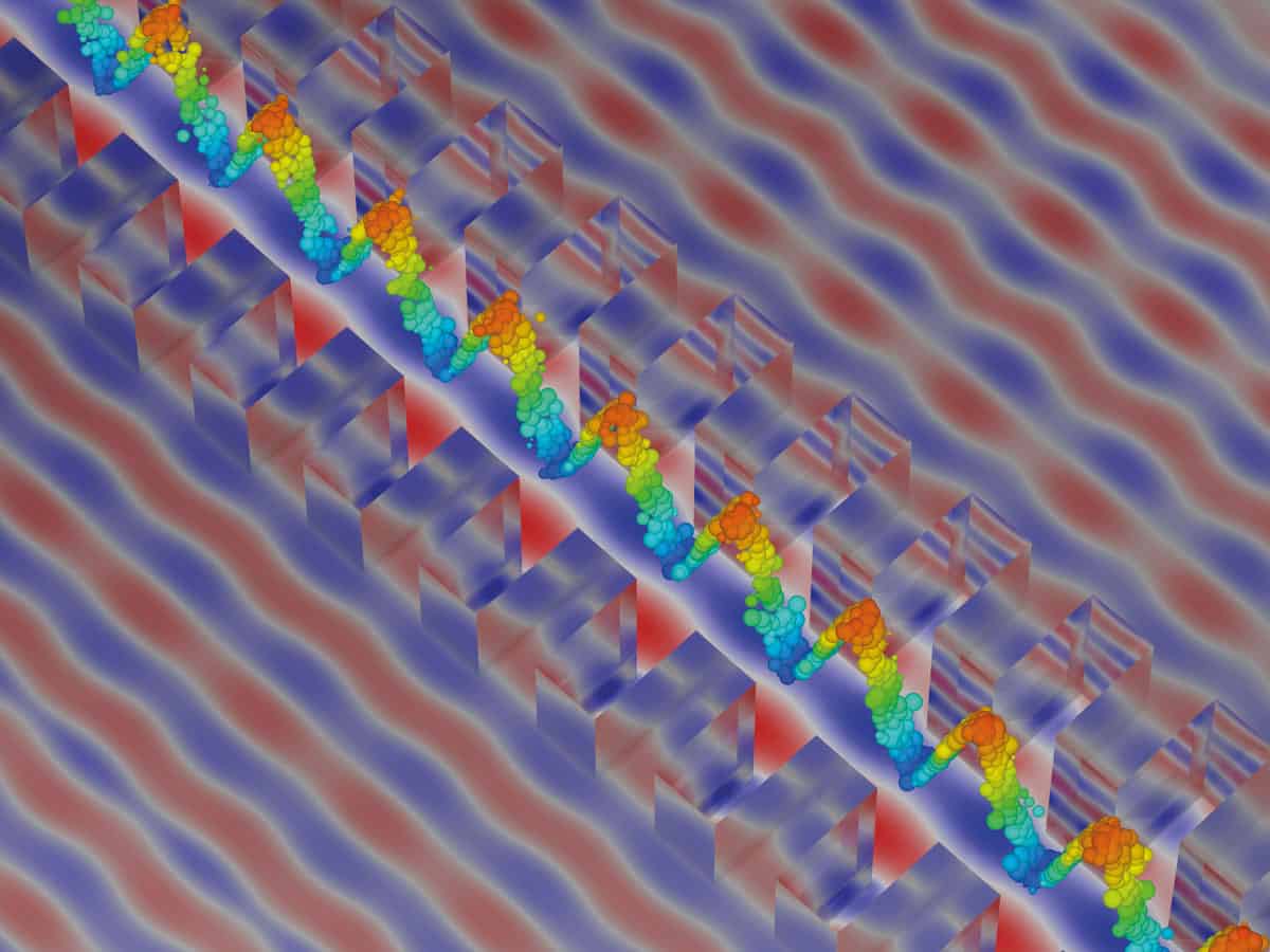
The first demonstrations of chip-based photonic accelerators were carried out by the SLAC–Stanford collaboration in 2013. Graduate students Edgar Peralta and Ken Soong, respectively, fabricated the prototype structures and developed the precision laser optics required to test them. Using photolithography, more than 200 individual accelerators were etched into a pair of bonded silica wafers. Each of the 1 mm2 devices contains a channel as narrow as 400 nm, into which are etched a sequence of ridges and gaps. When illuminated by a laser, these ridges shape the laser field to produce a wave that can impart energy to a particle that arrives at the appropriate time (see figure below).
Because most applications require particle accelerators to operate at relativistic energies, we designed the micro-accelerators to produce a wave that will continuously accelerate particles travelling at near-light speeds. To demonstrate the effect, individual structures were carefully aligned in the path of a pre-accelerated electron test beam at SLAC, while being illuminated by a titanium-sapphire laser. Because the particles arrived in bunches that were longer than the 800 nm wavelength of the laser, some were accelerated and some decelerated depending on whether they arrived at the peak or at the trough of the accelerating wave.
High gradients
Our initial tests last year demonstrated accelerating gradients as high as 300 MeV/m (Nature 503 91), but by further narrowing the width of the accelerating channel to enhance the accelerating field and using materials such as sapphire that can withstand higher laser intensities, it should be possible to increase the gradient by a factor of 10 or more. This would allow us, in principle, to shrink the entire 3 km-long SLAC linear accelerator to the size of a room, or to create lower-energy medical accelerators on a single wafer that would fit in your hand.
Alongside our ongoing experimental efforts, Peter Hommelhoff at Friedrich Alexander University in Germany and co-workers recently used an approach similar to ours to accelerate lower-energy (28 keV) electrons with gradients of 25 MeV/m (Phys. Rev. Lett. 111 134803). The German group is also developing ways to fabricate sub-micron-sized particle sources that can be triggered using the same laser that powers the accelerators. Such a particle injector would negate the need for a conventional radio-frequency accelerator on the front end of the microchip accelerator, as was necessary in our experiments, and is vital for making on-chip devices that can accelerate electrons to sufficiently high energies.
These first demonstrations of chip-scale accelerators are important steps, but a complete accelerator is still some way off. To reach useful particle energies, many of these tiny structures must be fabricated in succession and illuminated by a sequence of laser pulses that are precisely timed so that the particles see a continuous energy gain as they travel forward. The arrival times of the electrons and the laser must be synchronized to within a fraction of an optical period, corresponding to a few tens of attoseconds. This could be done, for instance, by introducing on-chip light guides with precise lengths that selectively funnel light into successive structures.
Another challenge is to avoid some of the particles being decelerated instead of accelerated. This requires that the incoming particles arrive in bunches that are separated by a distance equal to the wavelength of the laser and timed so that they all ride on the peak of the accelerating wave. Researchers at SLAC and Stanford have previously demonstrated a way to prepare the particles in this way using a laser to modulate the energy of the electrons followed by a magnetic compressor, which allows lower-energy particles to catch up with higher-energy ones. Accelerating these micro-bunched particles in unison at the peak accelerating field would also allow for monochromatic beams with a narrow energy spread, and we are now trying to integrate these approaches to design new particle sources that are optimized for testing micro-accelerators.
Similar techniques have been proposed to build a powerful source of pulsed X-rays for advanced crystallography research, for instance. By making on-chip laser-driven devices rapidly deflect rather than accelerate particles, a sequence of alternating deflectors in series would form an “undulator” that forces electrons to wiggle back and forth to generate bursts of synchrotron radiation. Such micro-bunched beams could potentially deliver X-ray pulses with durations of tens of attoseconds, allowing scientists to probe atomic and molecular dynamics on timescales three to four orders of magnitude shorter than present-day “conventional” X-ray free-electron lasers, such as the Linac Coherent Light Source at SLAC.
Industry appeal
We estimate that within the next 5–10 years tens of millions of electron-volts could be generated in an integrated device fabricated on a single 15 cm diameter wafer. To reach the billions or trillions of electron-volts needed for high-energy physics exploration, we will need to carefully align many such wafers in succession with sub-micron precision. This is straightforward when nanofabricating multiple devices on a single wafer, but more challenging if individual macroscopic objects are to be aligned. Consequently, in the next decade microchip accelerators will probably find their first applications in industry and medicine, where the required particle energies are in the much lower range of 1–20 MeV.
Companies that build accelerators for these sectors are beginning to express interest in commercializing the technology. Although the machines used in industry and medicine are smaller than high-energy colliders, they can still be the size of a room, weigh tens of tonnes and cost millions of dollars. Microchip-based versions could be sufficiently small and portable to allow endoscopic direct electron-beam cancer therapy, for instance. They could also enable more affordable medical X-ray sources for the treatment of clogged arteries, computed tomography (CT) scans and high-resolution imaging of biological tissues.
Similar devices for industry could provide a valuable X-ray source for non-destructive testing of products and materials, for instance by identifying cracks and deformations in hard-to-reach locations, or enabling new processes in the microchip industry by using multiple-beam X-ray lithography to rapidly “print” nanoscale patterns onto integrated chips. Accelerators for X-ray security screening of cargo and aircraft could also be made more widely available and, being smaller, capable of scanning larger areas or moving targets.
A number of these nearer-term applications are beginning to be explored and although the technology is not yet ready to compete with high-energy machines such as the 27 km-circumference Large Hadron Collider at CERN in Switzerland, it is clear that photonic devices are a promising approach for the future of particle acceleration.