As quantum computing enters the industrial sphere, questions about how to manufacture qubits at scale are becoming more pressing. Here, Fernando Gonzalez-Zalba, Tsung-Yeh Yang and Alessandro Rossi explain why decades of engineering may give silicon the edge

In the past two decades, quantum computing has evolved from a speculative playground into an experimental race. The drive to build real machines that exploit the laws of quantum mechanics, and to use such machines to solve certain problems much faster than is possible with traditional computers, will have a major impact in several fields. These include speeding up drug discovery by efficiently simulating chemical reactions; better uses of “big data” thanks to faster searches in unstructured databases; and improved weather and financial-market forecasts via smart optimization protocols.
We are still in the early stages of building these quantum information processors. Recently, a team at Google has reportedly demonstrated a quantum machine that outperforms classical supercomputers, although this so-called “quantum supremacy” is expected to be too limited for useful applications. However, this is an important milestone in the field, testament to the fact that progress has become substantial and fast paced. The prospect of significant commercial revenues has now attracted the attention of large computing corporations. By channelling their resources into collaborations with academic groups, these firms aim to push research forward at a faster pace than either sector could accomplish alone.
For these industry stakeholders, the question of what form a future quantum processor should take is particularly important. Unlike conventional microprocessors that manipulate information in binary bits, a quantum processor uses qubits: two-state systems that obey the fundamental principles of quantum mechanics. For example, each qubit can be prepared in an arbitrary superposition of two binary states. Hence, in contrast to classical bits that must always be either 0 or 1, a qubit may exist in a complex linear combination of 0 and 1. It is also possible to create selective correlations between different qubits. This property is known as quantum entanglement, and it lies at the heart of the exponential speed-up found in several quantum computing algorithms.
In principle, there are lots of ways to construct qubits. Some advanced prototypes use qubits made of a few dozen ions of rubidium or ytterbium, trapped in a vacuum chamber by time-varying electromagnetic fields. Other systems use lithographically patterned superconducting circuits kept at millikelvin temperatures in dilution refrigerators. Recently, however, experimental breakthroughs in silicon-based nanodevices have brought a third option to the fore. This option is, in effect, to manufacture quantum processors in the same way as conventional microprocessors, by leveraging widely deployed industrial complementary metal-oxide-semiconductor (CMOS) technology.
A silicon quantum computer
The idea of using silicon-based CMOS technologies to build quantum computers was first proposed in 1998 by Bruce Kane, who was then a researcher at Australia’s University of New South Wales (UNSW). In his paper, Kane suggested that arrays of individual phosphorus atoms in crystalline silicon could store qubits in nuclear spins, and that these spin qubits could be read and manipulated using nuclear magnetic resonance techniques.
Kane’s work (and that of other scientists who built on his ideas – see box below) attracted attention within the computing industry for several reasons. The first reason is a consequence of the relentless, Moore’s law-driven miniaturization of silicon devices. Thanks to decades of innovation, it is now possible to make transistors that are only few tens of atoms long. At this scale, however, quantum physics effects begin to prevent transistors from performing reliably – a phenomenon that limits prospects for future progress in conventional computing. This impending end to Moore’s law has prompted researchers in the field to consider new uses of silicon technology in a drive towards “more-than-Moore” electronics.
Another reason for the focus on silicon stems from the properties of the material itself. Noise is one of the great bugbears of quantum information processing, because it can make qubits change state at times and in ways that programmers did not intend, leading to computational errors. Most interactions with the surrounding environment, such as charge instabilities and thermal fluctuations, are sources of qubit noise. All of them can compromise information. Silicon, however, offers a relatively noise-free environment where spins can retain their quantum nature. The major source of unwanted quantum bit errors in silicon transistor-based qubits comes from the nuclear spins of silicon-29, a naturally occurring isotope present in all commercial silicon wafers. Luckily, purification methods can remove this unwanted isotope before the silicon crystals are grown, producing wafers of mostly spin-free silicon-28. For this reason, electron spins in silicon are among the most robust solid-state qubits available.
Perhaps the biggest attraction of silicon-based quantum processors, however, is that at their heart, they use the same technology that the microchip industry has handled for the past 60 years. This means manufacturers can expect to benefit from previous multibillion-dollar infrastructure investments, keeping production costs low. Just as importantly, using silicon as a basis for a quantum computer means that all the clever engineering and processing that went into developing modern classical microelectronics – from dense device packaging to integrated interconnect routing – can be adapted and used to build quantum devices.
On a grand scale
Having this solid engineering foundation will be a major advantage in efforts to overcome one of the biggest challenges in quantum computing: real-time correction of qubit errors. Even in relatively non-noisy systems, qubit errors cannot be entirely avoided, and the process of correcting them (known as a surface-code protocol) depends on a principle known as “qubit redundancy”. The basic idea of qubit redundancy is that one can construct a reliable logical qubit from a collection of noisy, error-prone physical qubits. The number of physical qubits required for each logical qubit depends strongly on the qubits’ error rate, but it could range from as low as a few tens to several thousand.
The error tolerance of qubits built in this fashion makes it possible for the whole quantum system to function correctly. Unfortunately, it also means that a truly powerful quantum computer will require millions of individually controlled physical qubits. Given that today’s most advanced quantum processors contain a few dozen qubits at best, implementing surface-code protocols in future machines will be challenging, to say the least. Issues with device-to-device variability, multi-layer electrical wiring and the need to couple quantum devices to classical control electronics all create headaches for quantum engineers. Before we can scale from a single, isolated pair of qubits to the hundreds of interconnected qubits required to perform calculations in a way that supersedes classical computers, these challenges will need to be overcome.
Researchers’ initial approach to this problem has been to produce concepts and blueprints of what a large-scale quantum computer could look like in silicon. Interestingly, most of these proposals suggest that a future silicon quantum processor should be composed of two layers.
The first layer would be a “quantum layer” in which 106–108 qubits are distributed in a square grid and allowed to interact with their nearest neighbours. This physical arrangement ensures that error-correction protocols can be performed efficiently, and the predicted number of qubits is in line with estimates of the resources necessary to run the most complex quantum algorithms designed to date. The large numbers involved suggest that very large-scale integration (VLSI) silicon technology, which enables chip manufacturers to place billions of components on an area the size of a fingertip, will be needed to create this quantum layer.
The second layer would be a “classical layer” composed of digital and analogue circuits that operate at cryogenic temperatures alongside the quantum processor. The role of this classical layer is not to process the quantum information. Instead, it would measure and control the qubits in situ, ensuring fast feedback between the two layers.
The vision for this two-layer device is clear: a quantum computer that can be manufactured using existing industrial processes, and then integrated with conventional electronics so that everything happens within the same silicon chip. Such a device would truly represent the best of both worlds, and it may also be necessary for solving the so-called input/output (I/O) problem.
Advancing the state of the art
Following Kane’s seminal work, UNSW scientists continued to develop silicon-based quantum technology. They demonstrated (in 2012 and 2019, respectively) that single-qubit and two-qubit logic operations could indeed be carried out using phosphorous atoms. They also showed that qubits could be made by confining single spins in nanometre-size regions of the silicon chip known as quantum dots (QDs). The quantum dot approach is considered more practical than Kane’s original idea because it does not rely on atoms being positioned very precisely in an array. Instead, lithographic techniques are used to arrange the gate electrodes so that the QDs exist in a well-defined pattern.
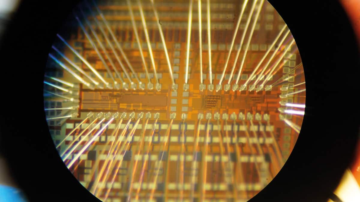
Silicon devices of this type do not, however, fully meet the stringent criteria for CMOS compatibility. In particular, the process of making the qubits employs techniques such as electron-beam lithography and scanning tunnelling microscopy that are considered unconventional within CMOS manufacturing. With this in mind, scientists at CEA-LETI, a technology research institute in Grenoble, France, took a different approach. They built a qubit device with an industry-standard fabrication process based on 300 mm silicon-on-insulator wafers. The CEA-LETI device, which the researchers developed as part of the European research consortium MOSQUITO (www.mos-quito.eu), consists of a nanowire transistor with an undoped channel and wrap-around gate electrodes. At low temperatures, two QDs form in the upper corners of the nanowire in which individual spins can be trapped (see figure right). Under the effect of a magnetic field, the electron spins align parallel or antiparallel to the field direction, producing the necessary quantum binary states. The need for two QDs arises because one is used to host a qubit, while the other one is used as a sensor to readout the qubit state.

Thanks to these experimental advances, silicon has cleared all the hurdles required to become competitive quantum-computing technology. The qubit fabrication process is scalable, meaning that mass-production is not only technically viable but also cost-effective. Qubits can be initialized and read out reliably, meaning that they can be reset before starting a computation and, at the end of it, their final state (the result) can be known. Information can be written them in on controlled way, and the qubits retain this information for long enough to perform operations.
These specifications are not too dissimilar from what one would ask of a classical computing technology, but silicon also makes the grade on another, uniquely quantum front. In 2018 researchers at Delft University of Technology in the Netherlands demonstrated that silicon-based qubits can be entangled controllably and with sufficient precision that, even if errors occur while the quantum processor is operating, users should be able to correct them using error-correction protocols. This led to the first programmable two-qubit quantum processor in silicon, which is currently the most advanced in this material.
To understand this problem, it is important to realize that qubits in today’s quantum-computing devices must be wired up one-by-one. This works well when the number of qubits is small, but as the technology develops, it will become impractical for cryogenic systems to support individual wires connecting room-temperature electronics to one million qubits at millikelvin temperatures. Fortunately, techniques from classical electronics offer a solution. In a modern microprocessor, billions of transistors on a chip are controlled efficiently by only a few thousand input and output lines. Hence, in silicon qubits (and indeed in qubits in general, regardless of their physical architecture), scientists and engineers will need to learn how to adapt concepts such as crossbar architectures and signal multiplexing to minimize the number of I/O lines.
Researchers have already performed some proof-of-concept tests indicating that the I/O problem can, in principle, be overcome. However, some specific hurdles remain. The first and possibly the most challenging concerns variability in the properties of quantum devices. Current proposals for large-scale quantum computing assume some level of shared control between qubits to mitigate the I/O problem. Implicit within this is the need for qubits to have a concrete level of uniformity between them, and for this uniformity to be achieved at scale.
In some respects, VLSI technology, thanks to its focus on minimizing the impact of process variation, guarantees a level of reproducibility that no other industry can provide. However, in the quantum realm, variability acquires a much higher degree of importance. Even a single atomic-level defect (for example in the quality of the interfaces or the purity and crystallinity of the material) may lead quantum devices to perform very differently. To accommodate this, the computing industry will need to develop strategies that go beyond the current state-of-the-art for silicon technologies – perhaps by constructing machine-learning models that anticipate qubit performance from room-temperature diagnostic data.
A second hurdle is to integrate CMOS electronics and silicon-based qubits into a single, monolithic chip. Although both technologies can be manufactured using existing silicon industrial processes, these processes currently involve different technological nodes; that is, they employ slightly different processing standards and protocols at the manufacturing stage. A common “classical-quantum” node will have to be developed and consolidated to produce hybrid quantum circuits at scale.
Full integration also implies that both technologies will have to operate at the same temperature. This problem is non-trivial given that qubits operate better at deep cryogenic temperatures (a few millikelvin), while the current models for integrated-circuit design are rarely accurate for temperatures below 20 K. Understanding the behaviour of silicon transistors (either as digital or as analogue circuit elements) at millikelvin temperatures will require a development effort of its own. To support that effort, researchers will need to develop precise models that can be imported into existing electronic computer-aided design tools.
The fact that millions of these elements will have to operate dynamically at these temperatures will also put tight restrictions on power budgets. The available cooling power in cryogenic environments is limited to a few hundreds of microwatts. Hence, the old strategy of simply sending a flow of cooling water around your processing unit is completely out of the picture.
While electrical engineers work to push the operation temperature of cryo-CMOS circuits down, physicists are working to understand how elevated temperatures affect qubit operation. There is optimism that these parallel efforts will produce an intermediate range of operating temperatures, one that will ease the burden on the CMOS industry while also enabling a higher power budget for the dynamical operation of the processor.
A collaborative future
Silicon-based quantum computing has come a long way since the late 1990s. The idea of taking conventional transistors and using them interchangeably as qubits or control devices on the same integrated circuit could, in the long run, prove viable both technically and commercially. The commercial promise of such a device means that research in the field extends beyond the traditional boundaries of university laboratories and into the research centres of global corporations such as Intel and Hitachi, both of which have long-standing collaborations with academic hubs in quantum computing.
It is still too early to say whether silicon will provide a path to the much sought-after general-purpose quantum machine. What is clear, however, is that it is a solid candidate eagerly backed by an industry that is keen to reinvent itself in a post-Moore’s-law future.