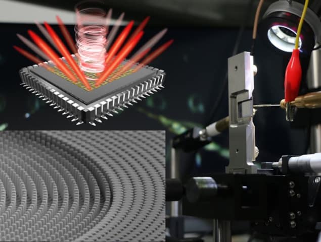
Vertical-cavity surface-emitting lasers (VCSELs) have emerged as a highly versatile light source over the past 30 years, with applications in areas from optical communications to instrumentation, manufacturing and sensing. A team of researchers in France and China has now augmented the VCSEL’s capabilities by integrating a nano-patterned beam-shaping structure into each laser during wafer-scale processing. This approach could make it possible to create light wavefronts designed to order, and thus construct devices such as ultra-compact programmable laser-on-chip arrays with whatever beam profiles are required.
First proposed by Kenicha Iga from the Tokyo Institute of Technology in 1977, the VCSEL is an efficient class of laser that uses very little current. Because VCSELs can turn on and off at high speeds, they can transmit vast amounts of data quickly. They also emit a circular beam of light, which greatly simplifies the optics required to focus the beam. Both attributes make VCSELs attractive for applications in telecommunications, and in recent years their applications have broadened to include image recognition. The iPhone X, for example, contains three VCSEL chips that are integral to its facial recognition system.
Like other lasers, VCSELs contain a cavity in which light is generated and emitted to produce stimulated emission. This cavity is sandwiched between two mirrors that provide the optical feedback necessary for lasing. In VCSELs, however, the laser cavity is very small, at just a few microns thick. This small size gives the laser its switching speed, but it also makes it hard to precisely control the shape of the light beam emitted. This is because light diffracts around features the same size as its wavelength, which makes it difficult to resolve, and thus control, smaller details.
Metasurface continually shapes wavefront
Laser beam shaping – that is, redistributing the laser’s intensity across the beam’s profile – is important for applications such as laser machining or medical devices that require laser light shaped in only one axis. Researchers led by Patrice Genevet of the Centre de Recherche sur l’Hétéro-Epitaxie et ses Applications (CRHEA) at the University Côte d’Azur and collaborators at the Key Laboratory of Optoelectronics Technology at the Beijing University of Technology have now demonstrated a way to achieve this control in VCSELs using flat, ultra-thin optical structures called metalenses.
In conventional bulky optical components, such as thick lenses, light rays travel more slowly in the thicker, central regions than in the thinner, peripheral ones because of the smaller phase velocity of light in glass compared with air. This distribution of phase delays in the lens leads to light refraction and focusing.
Metalenses produce similar effects, but with a different mechanism. In the CRHEA team’s work, the metalenses are made from a semiconducting gallium-arsenide (GaAs) film patterned with nanometre-sized circular pillars. These “nanopillars” are separated by distances shorter than the wavelength of the light they are designed to shape, and they act like optical antennas, introducing spatially varying phase delays in the light rays that pass through them and moulding the light beam according to the desired profile. The result is a metasurface that can be tuned for specific wavelengths of light simply by changing the size, diameter and spacing between the nanoantennas.
Laser collimation
To collimate their laser, Genevet and colleagues used a metalens design containing antennas of different shapes and sizes. These antennas cause the phase delays to be distributed radially around the lens, such that light rays are increasingly refracted further away from the centre, thereby shaping and focusing the wavefront of the incident light.
Smartphone market pulls VCSELs into the mainstream
In their experiments, which are detailed in Nature Nanotechnology, the researchers fabricated VCSELs in a “back-emitting” configuration. They directly integrated the metasurfaces into the lasers by sculpting the bottom (substrate) surfaces of the lasers into them. The result, which they term a metasurface integrated (MS) VSCEL, means that the metalenses serve as purely passive beam-shaping elements – that is, they do not alter the laser’s properties in any way, and therefore do not compromise its performance.
Compatible processing
Genevet explains that the team’s technology can be easily applied to state-of-the-art wafer-level fabrication techniques for VCSEL devices, making it possible to create chips of programmable and directional laser sources. The metalenses themselves can be fabricated using standard electron beam lithography techniques, with reactive ion etching used to create the nanopillars.
In contrast to micro-lenses, the ultra-thin form, unique planar configuration and CMOS-processing compatibility of the metasurfaces makes them promising candidates for integrating into ultra-compact optoelectronic devices, he says. Indeed, the new MS-VCSELs could find use in a wide variety of applications, such as optical fibre communications, laser printing, smartphones, optical sensing, facial recognition, directional displays and ultra-compact light detection and ranging (LIDAR), he tells Physics World.


