The president of the Royal Microscopical Society, Mark Rainforth, tells Siân Harris how a renaissance in electron microscopy is driving materials research forward and leading to new nanotechnologies.
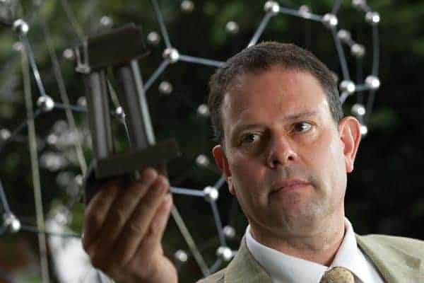
Mark Rainforth is professor of engineering materials at the University of Sheffield in the UK and has been involved with the UK-based Royal Microscopical Society (RMS) since he was a PhD student. His research involves using electron microscopy to study the interfaces and surfaces in metals, ceramics and coatings.
As president of the RMS since 2006, Rainforth oversees an organization that promotes every aspect of microscopy and allows all microscopists — users and instrumental developers alike — to interact. The society has over 1000 members including not just physicists, but also material scientists, life scientists, dentists and even archaeologists.
What have been the most exciting recent breakthroughs in electron microscopy?
There are so many that it is difficult to include them all. I remember going to a lecture a few years ago at which the speaker predicted that there was nothing exciting left to happen in microscopy and that all the changes would be incremental. In reality, over the past five years, the microscopy community has gone through a renaissance.
Perhaps the biggest advancement for me has been the ability to correct for the spherical aberrations that result from having round lenses. The resolution of a microscope has always been limited by such aberrations. People have known for a long time that the problems could be corrected by measuring the spherical aberrations and by using special lenses known as optipoles to put in equal and opposite aberrations. However, this requires many lenses and lots of image processing so has only really been possible with advances in computing power.
Before this it was only possible to produce an image that is a “projection” of atoms, rather than the actual individual columns of atoms in a material. Such a projection is made by recombining a number of diffracted electron beams to produce an interference image, which only under very carefully defined conditions gives us direct information regarding the atomic structure. Now, with aberration-free transmission electron microscopes, we can get true atomic images and get an idea of the physics of individual bonds between atoms.
In 1959 Richard Feynman famously said that, “It would be very easy to make an analysis of any complicated substance; all one would have to do would be to look at it and see where the atoms are…I put this out as a challenge: Is there no way to make the electron microscope more powerful?” Nearly 50 years later that challenge has been answered.
What other developments have been interesting?
The structures of many materials depend on their how atoms bond, something that must be studied at the angstrom (0.1 nm) length scale. But to understand how bonding affects what we can see with the naked eye, we must be able to make such measurements across much larger regions of a sample.
Electron back-scatter diffraction (EBSD) addresses this challenge by using a scanning electron microscope (SEM) to determine the crystal structure and crystal orientation of the atoms in a sample at the nanometre scale. The really exciting thing is that you can scan a wide area with SEM so you can cover a square centimetre of a material’s surface at nanometre-scale resolution.
This process is very computer-intensive and has only recently become possible with advances in computer power and digital cameras. Some of these latest techniques will be presented later this month in London at the Microscience 2008 conference.
Are these developments driving new science and technology?
Yes, but this is difficult to summarize because there are so many interesting cases. Indeed, it is almost like this renaissance has allowed us to revisit all known science.
Nanoscience and nanotechnology are widely recognized as having huge potential benefits. However, the technology cannot develop in a logical manner without the ability to probe atomic structure directly. This does not just mean the physical location of the atom, but also its atomic number and charge as well as the type of bonding with, and proximity to, surrounding atoms. Developments in microscopy are beginning to make this possible.
Microscopy also lets us manipulate objects on the nanoscale. For example, microscopes can be used to look at how a carbon nanotube can be moved into a specific position on a sample. In electronic components, we can now look at the interfaces between thin films and their substrates and understand the chemical distribution within the film. This understanding helps to further miniaturize the components leading to smaller mobile phones, for example.
Breakthroughs in microscopy have also boosted our ability to understand the effects of intentional or unavoidable trace elements in a material, which can dramatically alter its properties. Until the advent of the latest transmission electron microscopy (TEM) techniques, determining the locations of trace elements within the structure of a material was extremely difficult. Now, such microscopy techniques will, for example, bring new understanding in the degradation mechanisms in solid oxide fuel cells. Similarly, the development new high-strength, lightweight steels will also rely on the latest high-resolution techniques.
How is this renaissance in microscopy affecting your field of research?
My research focuses on the understanding of surfaces and interfaces. Microscopy underpins and explains all our work in materials science, be they metals, ceramics, coatings or biomaterials.
I use a range of techniques and sometimes need to combine more than one technique. For example, I use focused ion-beam microscopy to section surfaces for subsequent high-resolution TEM investigation. One situation where this is used is in examining the dynamic changes that occur in hip joint prosthetics while in the body.
What are today’s challenges in microscopy and how are they being addressed?
The current challenges cross many length scales, from achieving true atomic resolution, through to being able to find key features at the microscopic level, embedded randomly in a large object.
For atomic resolution, the first generation of aberration correctors have provided wonderful advances in resolution and therefore understanding. The next generation of (fifth-order) aberration correctors and chromatic aberration correctors, along with new electron gun designs, will in a few years’ time take the spatial resolution of electrons to a new level. Single atom electron spectroscopy should become almost routine. Such technology will also be built into SEMs, bringing major advances in the understanding of surfaces.
At the other end of the length scale, automatic stages coupled with advanced image analysis and related techniques, such as high throughput electron backscatter electron diffraction will bring major advances in the ability to resolve fine scale structure in a statistically meaningful way. Such techniques will benefit engineering firms that make large items with properties that are determined by fine-scale structure.
The rate of change is quite remarkable in every aspect. I am amazed by the number of new techniques coming out and I fully expect to continue to be amazed in the future. What better time to be a microscopist?
