A new atomically-thick strain sensor is 100 times more sensitive than commercial devices and 10 times more sensitive than alternative versions based on graphene. According to its developers at China’s Peking University, the prototype device, which is made from tungsten diselenide, could be used to make a new generation of electronic skin.
Tungsten diselenide (WSe2) belongs to a family of crystals known as transition metal dichalcogenides (TMDCs). These two-dimensional, van der Waals layered materials have the chemical formula MX2, where M is a transition metal such as molybdenum or tungsten and X is a chalcogen such as sulphur, selenium or tellurium.
In their bulk form, TMDCs act as indirect band-gap semiconductors. When scaled down to monolayer thicknesses, however, they behave as direct band-gap semiconductors, capable of absorbing and emitting light at high efficiencies. This property means that TMDCs in their 2D form are attractive building blocks for devices such as light-emitting diodes, lasers, photodetectors and solar cells. They could also be used to make circuits for low-power electronics and sensors. And unlike bulk semiconductors, which are usually brittle, TMDCs are able to withstand in-plane strains as high as 11%, which makes them promising materials for flexible electronic devices and strain sensors.
Nonlinear Hall effect
Researchers recently found that strain significantly affects the physical properties of TMDCs because it induces a form of magnetization when an electric field is applied. The result is a nonlinear version of the anomalous Hall effect in which the magnetic field exerts a sideways force on the material’s electrons, leading to a voltage difference proportional to the strength of the magnetic field and the longitudinal electric field. This is different from the conventional Hall effect, which occurs when electrons flow through a conductor only when an external magnetic field is present. The voltage produced also scales quadratically with the strength of the longitudinal electric field, in the absence of an external magnetic field, rather than linearly.
This type of Hall effect occurs when a Hall current is generated in response to a “second-order” component, which is related to the electrons’ orbital magnetism (that is, the magnetization induced by the particles’ orbital motion, rather than that caused by their spin), due to an applied electric field. It means that the charge carriers in a current travelling along a material can be deflected – thereby producing a Hall voltage without an externally applied magnetic field.
In 2019, researchers observed the nonlinear Hall effect for the first time in few-layer tungsten ditelluride, WTe2, a material that also belongs to the TMDC family of materials. Then, earlier this year, a team led by Zhi-Min Liao of Peking University’s School of Physics found it in a monolayer WSe2 when the material is strained along its crystalline axis.
Strain-resistance experiments
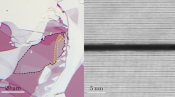
In the latest work, which the team report in Chinese Physics B, the researchers decided to investigate this effect further by studying how the resistance of WSe2 changes when strain is applied along the material’s crystalline axis. They performed their experiments on flakes of WSe2 obtained by shaving off monolayer-thin slivers from bulk crystals of the material. To apply strain in the direction they wanted, they selected flakes with long, straight edges and transferred these onto a single crystal piezoelectric substrate (PMN-PT). After they had aligned the WSe2 flakes along the [001] orientation of the PMN-PT crystal, they attached external electrodes to the flakes so that they could apply a voltage to the crystal to generate a piezoelectric displacement and induce strain in the WSe2 flakes in this direction.
Graphene-based strain sensor can detect a feather’s touch

By controlling the amount of strain applied, the team observed a so-called Berry curvature dipole, which is a quantum mechanical property that dictates how moving charges (such as electrons) propagate through solid semiconductors. With increasing strain, this Berry curvature dipole can generate an orbital magnetization, which decreases electron mobility and thus increases the material’s resistance. The researchers found that this resistance strongly depends on the strain applied in monolayer WSe2 at various temperatures and that the strain gauge factor (the ratio of the relative change in a material’s resistance to its mechanical strain – a key parameter of strain sensors) is as high as 2400 at 2 K.
The new work shows that the performance of strain sensors can be effectively improved by modulating the Berry curvature by changing the strain applied to 2D van der Waals materials like WSe2. “The technique should allow us to make highly sensitive strain sensors and flexible electronics,” Liao says. “The atomically-thick material is also easy to integrate into various nanodevices, which could be useful for nanoelectromechanical systems (NEMS),” he tells Physics World.