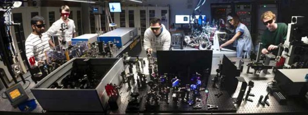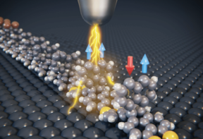
“Movies” of electrons as they move across a semiconductor junction have been made by researchers at the Okinawa Institute of Science and Technology in Japan using a new imaging technique. Combining photoemission electron microscopy with femtosecond laser pump-probe methods, the technique tracks the motion of electrons on timescales shorter than 1 ps. The researchers say it could provide a better understanding of how semiconductor devices work and lead to more efficient solar cells.
Solar cells – along with diodes, transistors and other semiconductor devices – rely on the flow of electrons across “heterojunctions” between two different types of semiconductor. While this motion is crucial to just about every modern technology, it is not easy to image in real time. The problem is that pulsed laser techniques – which can measure the energy of electrons on very short time scales – do not offer high enough spatial resolution to track the electrons. On the other hand, electron microscopy techniques offer high spatial resolution, but cannot keep up with the fast-moving electrons.
Best of both
Now Keshav Dani, Michael Man and colleagues have unveiled a new technique that combines high spatial resolution with high temporal resolution. Their method uses the well-established “pump-probe” technique involving laser pulses that are only 200 fs in length. It involves first firing a relatively intense probe pulse at a sample in the form of an indium selenide/gallium arsenide heterojunction that functions as a solar cell. The probe pulse plays the role of sunlight, putting electrons into excited energy states from which electrical energy can be extracted.
About 1 ps after the pump pulse, an image of the excited electrons is taken by firing a less intense probe pulse at the heterojunction. This ejects some electrons from the semiconductor, carrying with them information about the excited electrons in the semiconductor. These ejected electrons are captured and studied using spectroscopic photoemission electron microscopy, which creates an image of the electrons in the semiconductor.
Variable delay
By varying the delay between the pump and probe pulses, the team acquired a series of images of the excited electrons with a spatial resolution of about 250 nm and a temporal resolution of less than 1 ps.
This is a new door to understanding the motion of electrons in semiconductor materials
Keshav Dani, Okinawa Institute of Science and Technology
“We have made a video of a very fundamental process: for the first time we are not imagining what is happening inside a solar cell, we are actually seeing it,” explains Dani. “This is a new door to understanding the motion of electrons in semiconductor materials”.
When creating a solar cell, it is important that the electron excited states endure for long enough for energy to be extracted from the semiconductor. The images revealed that the lifetimes of excited electrons varied throughout the sample, with thinner regions of the semiconductor sample having faster decay rates. The images also suggested that electrons get trapped in thicker regions of the sample – something that could affect the performance of solar cells.
The new technique is described in Nature Nanotechnology.


