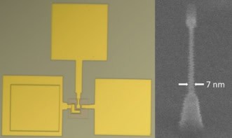
This year marks 20 years since Stephen Chou, Peter Krauss and Preston Renstrom first published their work showcasing a versatile approach for mass production of identical nanostructures for the electronics industry. This technique is called nanoimprint lithography and it involves pressing a nano-patterned structure into a hot molten polymer. As the polymer cools, the pattern stamped into it sets so that it can be used as a mould to make several identical replicas of the original structure.
Just as the printing press brought literature to the masses, it is easy to imagine how this nanofabrication technique could have a significant impact on the production of integrated circuits. To commemorate the development, Nanotechnology has published a perspective article on the technique, and I had a chance to talk to the author Qiangfei Xia of the University of Massachusetts at Amherst about the technique’s advantages, challenges and outlook for the future.
Although there were ways to produce 10 nm-scale structures in the 1990s using electron beam (ebeam) lithography, “it was like writing by hand”, as Qiangfei Xia puts it, and large-scale fabrication was still a challenge. While there have been valiant attempts to align and control tens of thousands of ebeams simultaneously, it is a complicated process – a little like trying to write with thousands of pens at once – and the volume of data that needs to be handled is colossal. Nanoimprint lithography may provide a more ready means for scaling up the production of these tiny structures.
The technique also helps to alleviate some of the other limitations of existing techniques. Xia describes asking Chou, who was his PhD supervisor back in the day, why he came up with the technique and it turns out that a lot of the motivation came from frustrations at the tiny changes in a nanostructure over time – nanoimprinting introduced a means of readily producing exact replicas. It can also be used on substrates that are electric conductors, which are prone to charging when using electron-beam fabrication processes.
Xia’s perspective in Nanotechnology describes some of the more recent developments for commercially competitive fabrication scales, such as roll-to-roll nanoimprint lithography. Whether the integrated circuit (IC) industry embraces the technique in its core manufacturing remains to be seen. Xia suggests that existing IC infrastructures have now reached a highly sophisticated level, and there is arguably little room for profit by making the changes needed to introduce nanoimprint lithography. However, for emerging technologies such as those used in the hard-drive industry, nanoimprint lithography may have a lot to offer.
Hear Xia describing the impact of nanoimprint lithography on nanotechnology in an audio feature on nanotechweb.org.