An innovative fin-shaped design for light-emitting diodes (LEDs) could not only overcome the devices’ limited brightness, it could also help turn them into lasers. The new scheme, from researchers in the US, could prove valuable in applications including chemical sensing, hand-held communication technologies, high-definition displays and disinfection.
Wide bandgap semiconductor LED technology has developed substantially over the last few decades and is now in common use – for general lighting and displays, but also for a range of applications in areas such as photodetection and optoelectronics. The technology does, however, suffer from a major drawback: as an LED’s current density increases, its internal quantum efficiency (IQE) declines.
This decline in efficiency means that although an LED shines more brightly when supplied with stronger electrical currents, it does so only up to a certain point. After that, its brightness begins to drop off – a phenomenon known as efficiency droop. The extra heat generated in the LED as the applied current increases exacerbates the problem, with IQEs dropping by about 30% as the temperature increases from 23° to 177°C. As a result of these effects, the power of LEDs with an area less than a square micron tops out in the nanowatt (nW) range.
Two mechanisms are believed to contribute to efficiency droop. In the first, known as non-radiative recombination, excited charge carriers (electrons and holes) recombine without emitting light. This unwanted process lowers the efficiency of light generation and increases heat losses, since the electrons and holes recombine by producing phonons – thermal vibrations of the crystal lattice – instead of photons. In the second mechanism, known as Auger recombination, the energy of the electron-hole pair is transferred to another electron or hole, again without a photon being emitted. This charge carrier then normally loses its excess energy to thermal vibrations.
Tiny comb
The new LED design, which was created by researchers at the National Institute of Standards and Technology (NIST), the University of Maryland, Rensselaer Polytechnic Institute and the IBM Thomas J Watson Research Center, had a serendipitous start. The research team did not set out to solve the efficiency droop problem directly. Instead, they were exploring ways of creating micron-sized LEDs for applications such as a miniaturized lab-on-a-chip.
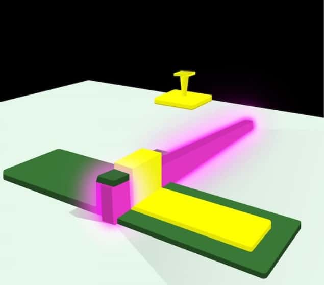
NIST team member Babak Nikoobakht, who conceived the new design, explains that he and his colleagues used the same materials as in conventional LEDs, but formed into a different shape. Unlike the flat, planar design commonly used, Nikoobakht and colleagues built their light source out of long, thin zinc oxide (ZnO) strands, or fins, measuring around 5 microns in length and approximately 160 nanometres in width. The resulting fin LED array, grown on a gallium nitride (GaN) substrate, looks like a tiny comb that extends over areas as large as a centimetre or more.
“We saw an opportunity in fins, as I thought their elongated shape and large side facets might be able to receive more electrical current,” Nikoobakht says. “At first we just wanted to measure how much the new design could take. We started increasing the current and figured we’d drive it until it burned out, but it just kept getting brighter.”
The group’s new ZnO-GaN fin LED emits light at violet to ultraviolet wavelengths and generates about 100 to 1000 times as much power as a typical micron-sized LED – up to 20 mW. The new design does not exhibit efficiency droop, even at record-high current densities of 1000 kA/cm2. Measurements of the device’s total spectral radiant flux also show that its output power increases linearly with drive current.
“One of the most efficient solutions”
Grigory Simin, a professor of electrical engineering at the University of South Carolina, US, who was not involved in the project, says that the new design is one of the most efficient solutions he has seen. “The community has been working for years to improve LED efficiency, and other approaches often have technical issues when applied to submicrometre wavelength LEDs,” he comments in a NIST press release. “This approach does the job well.”
Nikoobakht and colleagues also discovered that as they increased the current supplied to the LED to 1000 kA/cm2, the LED’s comparatively broad-band emission light (with a wavelength in the ultraviolet range, around 385 nm) narrowed to just two wavelengths (403 and 417 nm) of an intense violet colour. At this point, the device started to lase with a brightness of over 20 mW.
Polymer LEDs go nano
According to the researchers, their nanoLED’s enhanced light-emitting performance comes from the fin shape mitigating nonradiative pathways. The large side facets of the fins also allow for effective electrical injection and form a laser cavity.
Nikoobakht notes that converting an LED into a laser usually requires a lot of effort, and typically involves coupling the device to a resonance cavity that allows the light to bounce around and increase in intensity. In this case, however, “it appears that the fin design can do the whole job on its own, without needing to add another cavity,” he says.
While the nanoLEDs and nanolasers described in this work operate in the near UV range, the researchers say their concept could be applied to different materials systems, such as aluminium gallium nitride (AlGaN), boron nitride (BN) or their heterostructures, to develop far brighter deep-UV devices. They report their work in Science Advances.

