A new 2D material just one atom thick has been made by an international team of researchers led by Axel Enders. Dubbed hexangonal boron–carbon–nitrogen (h-BCN), the material could offer many of the benefits of graphene, which is a hexagonal lattice made of just carbon. But unlike graphene, h-BCN has a direct electronic band gap, which could make it useful for creating electronic devices.
First isolated in 2004 by Andre Geim and Konstantin Novoselov, who shared the 2010 Nobel Prize for Physics for their discovery, graphene is blessed with a wealth of potentially useful mechanical and electronic properties. Despite being so thin and flexible, graphene is much stronger than steel and is an excellent conductor of heat. Graphene also conducts electrons at extremely high speeds. As a result, it could be the ideal material for making electronic devices that are ultrafast, high-density and even bendable.
Mind the gap
Many of graphene’s electronic properties arise from the fact that it is a semiconductor with a zero-energy gap between its valence and conduction bands. This is not ideal for making transistors and other electronic devices because such circuits need semiconductors, such as silicon, that have a band gap. In an attempt to make a modified version of graphene that does have a band gap, device developers have therefore explored various schemes – including applying an electric field, adding chemical impurities or modifying the structure of graphene. None, however, has proved ideal.
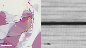
Now, Enders and colleagues at the University of Bayreuth, University of Nebraska-Lincoln, University of Krakow, State University of New York at Buffalo, Boston College and Tufts University have developed a graphene-like material that could fit the bill. The team made h-BCN by heating an organic molecule containing boron, nitrogen and carbon on an iridium substrate. The result is an atomically thin layer of h-BCN that is corrugated because of the lattice mismatch between the layer and substrate.
Multiple techniques
The team studied the structure and electronic properties of the film using molecular-resolved scanning tunnelling microscopy imaging, X-ray photoelectron spectroscopy and low-energy electron diffraction. The researchers also used density functional theory and first-principles calculations to further understand h-BCN.
An important result of the measurements and calculations is the prediction that h-BCN should have a direct electronic band gap of a size that falls between that of gapless graphene and hexagonal boron nitride, which is an insulator. According to the researchers, this band gap could make the material better suited than graphene for electronics applications.
“Our findings could be the starting point for a new generation of electronic transistors, circuits and sensors that are much smaller and more bendable than the electronic elements used to date,” says Enders. “They are likely to enable a considerable decrease in power consumption.”
The study is described in ACS Nano.