Physicists in Germany have developed a new approach to atom lithography that can beat the classical diffraction limit by a factor of two. The technique, developed by Markus Oberthaler and colleagues at the universities of Heidelberg and Konstanz, exploits quantum aspects of the interaction between light and matter (D Jürgens et al. 2004 Phys. Rev. Lett. 93 237402).

Standard approaches to atom lithography employ off-resonant standing waves. However, the diffraction limit of light restricts the minimum feature size that can be fabricated with this approach to about half the wavelength of the laser beam used to create the standing wave. Oberthaler and colleagues have now shown that nanostructures with smaller feature sizes can, in principle, be fabricated if the laser beam is resonant with an electronic transition in the atoms.
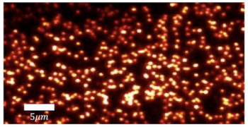
The experiment involves passing a tightly focused beam of chromium atoms through a resonant standing wave, which is produced by reflecting a linearly polarized laser beam from a mirror (figure 1). After passing through the standing wave, the chromium atoms are deposited onto a silicon substrate and the resulting pattern is analysed with an atomic force microscope (AFM).

The Konstanz-Heidelberg team found that nanostructures with feature spacings of half the wavelength of the laser light were produced when the laser was tuned far from its resonance frequency. However, when the laser was almost resonant with a transition in the chromium atoms, a complex structure containing additional features – each separated by a quarter of the wavelength of the laser light – was seen (figure 2).
According to the team, these features are produced by quantum interactions between the atoms and the laser beams, and by the quantum motion of the atoms. “The most significant impact of this work is the ‘direct’ observation of quantum mechanical atom-light interaction properties,” Oberthaler told PhysicsWeb. “However, the experiment has also shown that the combination of deposition and AFM allows us to study quantum motion on the nanometre scale.”