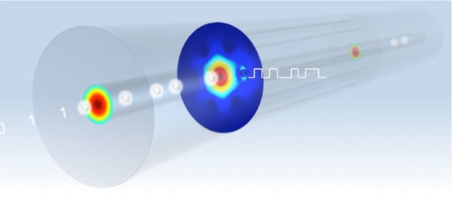
An international team of researchers has integrated a semiconductor junction into an optical fibre for the first time. The device, which works at gigahertz frequencies, is the first step in creating an all-fibre optical-communications network where light is generated, modulated and detected within a fibre itself without the need for integration with electronic chips. Its range of applications could run from improved telecommunication systems and laser technology to more-accurate remote-sensing devices.
The research team, led by John Badding, a chemist at Penn State University, includes other chemists at Penn State and a team of physicists at the Optoelectronics Research Centre at Southampton University in the UK.
Fibre to wire, and back
One of today’s crucial technological challenges involves developing a way to seamlessly and rapidly exchange information between optical systems and electronic ones. Badding explains that when it comes to existing technology, the merging of a round optical fibre with the minute components on a flat electronic chip is difficult to achieve. But integration is crucial because silicon-based integrated circuits are the building blocks for most electronic devices.
“For example, light is transmitted from London to New York via fibre-optic cables when two people set up a video call on their computers. But the computer screens and associated electronic devices have to take that light and convert it to an image, which is an electrical process. Light and electricity are working in concert in a process called an OEO conversion, or an optical–electrical–optical conversion,” says Badding. Instead, Badding and other researchers around world are trying to find an “all-fibre solution” where the electrical components can be directly integrated into an optical fibre such that the light never needs to leave the fibre.
But that is easier said than done. In addition to the challenge of shaping a connection between flat chips and round fibres, a major problem is the size of the objects involved. “An optical fibre is 10 times smaller than the width of a human hair. On top of that, there are light-guiding pathways that are built onto chips that are even smaller than the fibres by as much as 100 times, so imagine trying to line those two devices up,” Badding explains.
Novel merger methods
Instead, the researchers have come up with a novel way to integrate the two components: they built a new kind of optical fibre that contains its own integrated electronic component. They used a high-pressure chemistry technique known as “chemical vapour deposition” to deposit layers of semiconducting materials directly into specially fabricated tiny pores in an optical fibre. By doing so, they effectively create a semiconductor junction inside a fibre. “We had to rethink basic semiconductor fabrication, only within an optical core,” says Badding.
The researchers began with an empty pore in an optical fibre and then added layers of platinum and doped silicon, creating the junction. Badding points out that an added benefit of the technique is that it uses silicon – “the classic material of modern electronics”. The main challenge was to layer the semiconductor materials evenly on such a long, thin hole. “People were surprised that our method worked because the holes are so long and thin…they kept asking us why the hole did not clog,” says Badding. But he explains that they used extremely high pressure – more than 300 times greater than the atmospheric pressure – to deposit one layer, which is then heated and then another layer is painted onto the first, creating the junction. “It’s like trying to evenly and smoothly painting a garden hose that runs from say London to Southampton,” he claims.
All-fibre networks
In the end the team was successful and the researchers produced, for the first time ever, an integrated optoelectronic fibre. Their method is also cost-efficient, as it does not require the multimillion-dollar clean-room facilities and equipment that conventional chip fabrication demands. Other benefits of the method include the fact that the technique could work quite well with other semiconducting materials.
In the future, one of the key goals of research in this field is creating an all-fibre network. “If the signal never leaves the fibre, then it is a faster, cheaper and more efficient technology,” says Pier Sazio from the University of Southampton, who is one of the team’s leaders. “Moving technology off the chip and directly onto the fibre, which is the more natural place for light, opens up the potential for embedded semiconductors to carry optoelectronic applications to the next level. At present, you still have electrical switching at both ends of the optical fibre. If we can actually generate signals inside a fibre, a whole range of optoelectronic applications becomes possible.”
The work is published in Nature Photonics.


