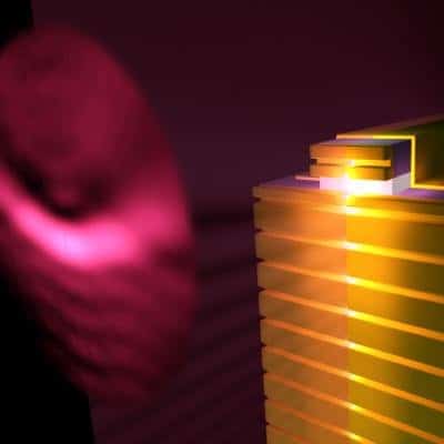
Researchers in the US and Japan have devised a simple way generate a nearly parallel beam of light from a semiconductor laser — without the need for bulky and expensive lenses. Instead, a patterned metallic film is used to absorb divergent light from the laser and reemits it one direction. The team says that the technique – which relies on collective electronic excitations called “plasmons” — could make semiconductor lasers cheaper, smaller and more efficient.
Semiconductor lasers, which emit light when electrons combine with holes at a p-n junction, have been around for almost 40 years and can be found in everything from the sophisticated optical-communications systems that power the Internet to five-dollar laser pointers. Although semiconductor lasers are very small (some are micrometer-sized) and can be integrated within electronic devices, the light-emitting region of the laser is about the same size as the wavelength of the laser light. This means that the light emitted from the laser is diffracted, often by as much as several tens of degrees.
As most laser applications require a collimated beam with a much smaller divergence, the light is usually collimated by placing a high-quality lens with a large collection angle (or numerical aperture) at the laser output. Unfortuantely, that makes semiconductors more expensive and relatively bulky. Now, however, Nanfang Yu, Federico Capasso and colleagues at Harvard University in the US, along with researchers at the optical-equipment maker Hamamatsu Photonics , have collimated laser light by placing a thin, patterned metal film on the output facet of a semiconductor laser (Nature Photonics doi:10.1038/nphoton.2008.152).
Parallel grooves
The film has an aperture is a slit that is about 2µm wide which is adjacent to a series of parallel grooves that are 0.8µm wide, 1.5µm deep and separated by 8.9µm. The collimator was fabricated on the surface of a semiconductor laser that emits infrared light at a wavelength of 9.9µm.
Some of the laser light travelling through the aperture is absorbed, creating surface plasmons — collective excitations involving large numbers of electrons on the surface of the metal film. As the plasmons propagate across the film, they are scattered by the grooves, which results in the plasmons being converted back into light with the same wavelength as the laser.
The size of the aperture and grooves are chosen so that the remitted light undergoes constructive interference to form a beam of light that propagates outward and perpendicular to the laser facet.
The divergence of the plasmon-collimated laser was about 2.4o, whereas the divergence of the same laser before being fitted with the collimator was about 63o.
New dimensions
Although this collimator only works in one dimension, Yu said that the team are now working on a 2D design involving a circular aperture surrounded by concentric rings of grooves. “Preliminary results in our group have shown that this scheme works very well: a divergence of a few degrees in the horizontal and vertical planes has been achieved in a quantum cascade laser.” said Yu.
So far, the team has made their collimator lenses using two different methods. One technique involves depositing a 1.7µm layer of gold on the flat surface of the laser facet, and then using an ion beam to cut the grooves into the metal. The second technique used the ion beam to cut grooves into the facet of the laser, which was then coated with a 400 nm-thick layer of metal. Both techniques resulted in similar improvements in collimation.
Milling, however, is an expensive and time-consuming technique that is not suitable for mass production. The team is now looking to develop new ways of making the collimators that are more in line with commercial semiconductor fabrication techniques.
The team believes that their collimator design — which is the subject of a patent application — could someday be used to create compact, low-cost semiconductor lasers for use in optical sensors that use beams of laser light to detect chemicals in the environment, for example. The technology could also lead to lower cost optoelectronics devices. “A very narrow spread of the laser beam can greatly reduce the complexity and cost of optical systems,” said team member Hirofumi Kan of Hamamatsu Photonics.


