Tongtong Zhu is founder and chief executive of UK start-up Porotech, which makes micro-scale light-emitting diodes for full-colour displays. He talks to Margaret Harris about the technology’s development, the role of material defects, and the transition from academia to industry
So how did Porotech begin?
It all started from a research project in the Cambridge Centre for Gallium Nitride. I was working on single-photon sources for quantum communication, trying to make micro cavities to enhance the coupling between the emitter and the cavity. Probably the easiest micro cavity component is a Bragg mirror, but to make it reflective you need to get a refractive index contrast between different layers.
We could achieve the reflectivity with gallium nitride, but the defects – which you can’t get around – were hindering device performance. So we exploited some of the intrinsic dislocations, which are a common structural defect. Using wet chemistry, we formed a matrix of porous composite between gallium nitride and air. That mixes up the refractive index of the gallium nitride and the air, yielding a much wider parameter for tuning the optical properties.
After doing some business courses, developing a business plan and getting it critiqued, we were confident enough to move out of the university and commercialize our idea
We made the highest-performing single-photon sources in the blue spectrum, but obviously this reflectivity is also beneficial for all kinds of optoelectronics. To make a light-emitting diode (LED), you need the bottom mirror to reflect light and then be able to extract the photon. We tested it – and it worked beautifully. After doing some business courses, developing a business plan and getting it critiqued, we were confident enough to move out of the university and commercialize our idea.
You won a Business Start-up Award from the Institute of Physics in 2022 for making a red indium gallium nitride LED. What was the biggest challenge to that innovation – and how did you overcome it?
Red is not that difficult to achieve with other materials, like gallium phosphide or gallium arsenide. On paper, it should also be achievable with gallium nitride, in terms of the band gaps defined by the material. But defects are a problem – as you go to from blue to green and then even longer wavelengths, you need to put more indium in the light-emitting area, which makes the quantum wells thicker.
And the trouble with gallium nitride compared to many other compound semiconductors is that the lattice parameter mismatch is huge between different alloys. So you get a lot of strain, and if that’s not properly relieved, you will incur lots of defects that will hinder the LED’s performance. If you add more indium atoms, there is also a risk of phase separation, where they will just stay as metal platelets rather than forming crystalline materials.
We then build on top of this beautiful porous architecture so we can manipulate the material’s optical and mechanical properties. We can actually change the mechanical property and enlarge the lattice parameter in a simple way so that it can be more matched to the light-emitting area – the high-indium-content region that we are trying to build on top. The closer match we can get, the fewer problems we will encounter in the light-emitting area.
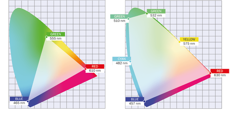
What are the implications of having a red indium gallium nitride LED alongside green and blue ones?
Blue and green are already very successful and established using gallium nitride, but industry currently has had to use other sources like gallium arsenide for the red. That’s really costly, both in terms of capital expenditure and throughput. What’s more, mixing different materials substantially reduces the yield, and subsequently the adoption rate as well. Getting all the colours from a single material means we can use the existing supply chain making blue and green and use them to generate red as well – without any additional capital expenditure or complications with the processing flow.
You’ve also made tunable wavelength emitters, what you call DynamicPixelTuning®. How do they work and alter the picture you just described?
It was an accident in a way. By extending the wavelength capability of gallium nitride to red, we found out we can actually also shift the colour to the other side of the spectrum. Fundamentally, with gallium nitride there is some internal strain, which really affects how the quantum wells and the band gap react when an external bias is applied. Everybody wants to achieve a stable single colour, but when you inject a current, that external bias will affect the internal field, varying the wavebands.
We can reduce the strain, which would improve the stability, but we can’t eliminate 100% of the internal field just by material manipulation. We wondered if we could capitalize on the strain status and enlarge that internal field, so when we apply an external bias, the shift is large enough that we can have all the colours. In fact, we can now achieve the large wavelength shift in a controllable way. It’s a very linear relationship, so you can have any colour as a function of the current density.
So we have two ways of approaching the market and working with existing capabilities, depending on the complexity of a customer’s system and their display requirements.


What’s next for Porotech? Are you looking to expand?
For us it’s very important to pull in customers on the one hand, but also to spread our risk. We don’t want to be betting on just one market segment, so we are looking at three major areas: large TV and signage; smart wearables; and AR/VR. With the first area, we’re talking about new high-end TVs with 100-inch displays, that no other existing technology can implement so cost-effectively.
Our technology can enable sense and touch functionality, which will help smart wearables to become more personalized items in future
As for smart wearables, we’re talking smart watches, goggles and glasses. The micro LED fundamentally is a display technology, but it’s building on top of the semiconductor ecosystem and the integration with silicon transistors, so it promises integrability and other functionality as well. It can give display information but can also enable sense and touch functionality, which will help smart wearables to become more personalized items in future.
For AR/VR we are also trying to contribute on top of the micro LED, the photon, the light output and the optoelectronics. We’re also focusing on the future integration with the silicon foundries and silicon transistors. Obviously that’s a lot harder because of the restricted weight and small volume that’s required for the AR/VR to be implemented on simple glasses.
So we are more commercially ready for the big TV and smart watches, but for AR it’s more about the system-level integration and engineering.
You started out as an academic, so it must have been a learning curve for you to learn how to talk about supply chains, capital expenditure and integrating your product with different devices
I’m still learning actually, and I’ve been quite happy taking on that challenge. I could have pursued academic excellence, but since we’re doing applied science and materials, we really have to focus on how to implement that to benefit industry and people. So I felt quite pumped-up initially, that I chose this route to new personal development.
Industry or academia? How to choose your path
You realize very early on you are less capable, less knowledgeable, and you don’t have any experience. You have to learn from other people. It was very good that the Cambridge ecosystem provides all that mentoring on top of the university support. That’s why we spent a couple of years hopping inside and outside the university, using some of the resources, doing market research and getting ourselves trained up.
Learning is an everlasting process as we continue to grow, but it is a very worthwhile investment.
Do you have any advice for people seeking to turn their technology into a commercial product?
My advice would be to listen more and talk less. Technology is good, physics is wonderful, but that’s only one-third or one-quarter of the problem. You’re going to need people, resources and a strategy for how to transfer the technology into a real product and get the business plan to support it. You’ll need to engage with a wider community to hear different views and critiques. Take that feedback and reflect on it to improve yourself and your ideas.
I think that’s a hard learning curve that everybody has to go through. But admitting that you are not capable of everything from the beginning, and learning from more experienced people is very important. One small company can’t do everything by itself. You need a lot of help from university, government, supply chain and customers and partners, even your family and friends. So listen more and reflect on a personal level. That’s what I would recommend.