Photoresponsive flash memories made from organic field-effect transistors (OFETs) that can be quickly erased using just light might find use in a host of applications, including flexible imaging circuits, infra-red sensing memories and multibit-storage memory cells. Researchers from Hanyang University in Seoul and Pohang University of Science & Technology (POSTECH) have now found that they can significantly improve the performance of these devices by making use of floating gates based on cadmium selenide (CdSe) quantum dots whose surfaces have been modified.
“OFET-type light-erasable memories have recently emerged as promising elements for information delivery,” explain Yong Jin Jeong and Jaeyoung Jang, who led this research effort. “The erasing process in this type of device is usually controlled using only light following a photo-induced recovery mechanism that works thanks to photo-induced charge transfer across the interface between a semiconductor and floating-gate layers in the device.”
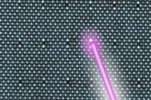
Photo-induced recovery after just one second
Jang and colleagues studied CdSe quantum dots whose surfaces they had covered with three different organic molecules that they used as photoactive floating-gate interlayers in light-erasable transistor memory architectures. They looked at how modifying the surfaces of the dots affected the performance of the memories and found that capping small ligands of octadecylphosphonic (ODPA) and fluorinated molecules improved the diffusion of holes between the dots and the conducting channels in the devices. This allowed for photo-induced recovery after just one second using low intensity light (with a power of 0.7 mW/cm2).
“We had made OFET memories before (containing a polymer/C60 composite floating-gate interlayer) that could also be erased using low-intensity green light (of 0.5 mW/cm2) and in which we could effectively remove trapped charge carriers (electrons and holes) and so recover the initial state,” says Jang. “These devices did suffer from several problems, however. The main one was that erasing stored information took as long as 30 seconds and read-out required a (destructive) applied gate voltage in addition to light.”
Fast erasing using low intensity light
“Employing tailor-made floating-gate materials for transistor memory devices overcomes these problems and allows for fast erasing using low intensity light (again, green) and a non-destructive read-out process. These gates perform many crucial tasks: they generate charge carriers (electrons and holes) when they absorb light and transfer these charges to the semiconducting layer in the transistor.”
Using quantum dots for the floating gates is much better than using C60 or other commonly employed materials, he adds. This is because the optical and electronic properties of these dots can be modified by engineering their particle size or adding surface ligands, as in this study.
The new devices boast high memory ratios of over 105 between OFF and ON bi-stable current states for over 10 000 seconds and good dynamic switching behaviour, he says.
Towards commercialization
The researchers believe that their light-erasable OFET memories could be commercialized in the near future and that their work could provide a “useful guideline” for designing photoactive floating-gate materials.
“To the best of our knowledge, we are the first to engineer the surface of quantum dot floating gates in such memories,” Jang tells Physics World. “Our proof-of-concept memory devices also consume less power during operation and could be integrated with highly sensitive photodetectors for use in flexible imaging, integrated sensors and biomedical applications.”
So, where next? The Korea researchers say they are now busy trying to develop quantum dot-based light-erasable memories using all-solution-based processes. “In our present experiments, we used vacuum-based techniques to deposit the organic (pentacene) semiconductor and (gold) source/drain electrodes when making our devices,” says Jang. “These are not suitable for large-area, low-cost applications, however, because they are expensive, time-consuming and complicated, so an all-solution process would be better.”
The new memories are detailed in ACS Nano 10.1021/acsnano.8b01413.