Available to watch now, WITec explores the principles of 3D Raman imaging
Want to learn more on this subject?
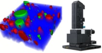
Raman spectroscopic imaging is a powerful, versatile and increasingly common microscopy technique that can quickly identify molecules in a sample and visualize their distribution in three dimensions. This fast, nondestructive and label-free chemical characterization method offers enormous potential to physicists in many fields of research.
Modular Raman microscopes can be integrated with advanced cooling stages for cryogenic measurements, with environmental enclosures for remote operation, and even within vacuum chambers for advanced structural analyses.
This presentation will describe the principles of 3D Raman imaging and the speakers will show in detail how to access chemical imaging at the highest spatial resolution.
Comprehensive analyses of samples often require a combination of different techniques. Structural information on a sample’s surface can be obtained by Atomic Force Microscopy or Scanning Electron Microscopy (SEM). Raman imaging can reveal its chemical composition and by combining the techniques, structural and chemical information can be easily acquired from the same sample position. These approaches will be described and the power of correlative Raman-AFM and Raman-SEM imaging for analysis will be illustrated in the contexts of 2D materials development, cryogenic research, pharmaceutical sciences, geosciences, battery research and life sciences.
Want to learn more on this subject?
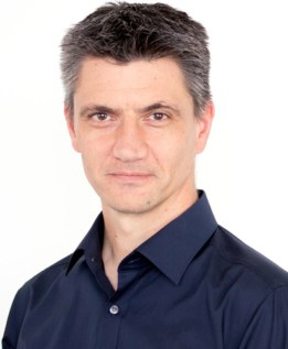 Thomas Dieing is technical product manager for the WITec alpha300 product line and its accessories. He obtained his PhD from La Trobe University, Melbourne, Australia, in 2005 investigating the MBE growth of nitrogen containing III/V semiconductors. In 2006 he joined WITec’s application team and became director of applications and support. In his role as product manager since 2019 he is responsible for all activities related to the product development process.
 Ute Schmidt studied physics at the Babes Bolyai University in Cluj-Napoca, Romania, and obtained her PhD from the University of Karlsruhe, Germany. Through her work with in situ scanning tunneling microscopy in an electrochemical environment, she was introduced to scanning probe microscopy. During her postdoctoral scholar position at Karlsruhe and North Carolina State University in Raleigh, USA, she continued to work with metal deposition on different substrates with STM and Atomic Force Microscopy. Schmidt worked for six years as a project manager at Molecular Imaging Corp., Phoenix, USA. She has been an applications manager at WITec since 2003.
