Commercially available lens correctors are extending the reach of electron microscopes to unprecedented atomic scales, as Peter Nellist describes
How many students are told, perhaps during their first science lessons at school, that atoms are too small to see? Indeed, with typical diameters of 10-10 m, atoms were for a long time considered articles of faith by many scientists. We cannot see atoms, we are later taught, because diffraction places a fundamental limit on the resolution of an image. Roughly speaking, we cannot see anything smaller than the wavelength of the light used to produce the image. And since the wavelength of visible light is some 10,000 times larger than the typical distance between two atoms, we cannot see individual atoms.
But other forms of electromagnetic radiation have much shorter wavelengths than visible light. The X-rays used in crystallography, for example, have wavelengths of less than a nanometre. The problem is that it is extremely difficult to focus X-rays. Luckily, quantum mechanics provides an alternative way to view the microscopic world: subatomic particles.
Quantum mechanics dictates that all particles have a de Broglie wavelength of λ = h/p, where h is Planck’s constant and p is the momentum of the particle. For example, an electron that has been accelerated to 0.78 times the speed of light has a de Broglie wavelength of 2 pm (2 × 10-12 m), which is about 100 times smaller than the typical interatomic distance in a solid. Moreover, because electrons are charged they can be deflected by electric and magnetic fields.
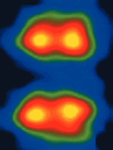
By combining such electromagnetic “lenses” with an electron gun, and adding some sort of electron-detection system, we have an electron microscope. For the last 70 years these instruments have provided researchers across numerous disciplines with valuable and often beautiful images of the ultra-small. Today, one of the world’s most powerful microscopes is capable of resolving individual atomic columns in materials such as silicon (see figure 1). This particular microscope, which is over 10 years old, was able to achieve this unprecedented level of resolution (about 78 pm) thanks to the commercial availability of special components known as “aberration correctors”.
Adding an aberration corrector to a microscope is like fitting it with a pair of glasses, allowing microscopes to see things that they could not see before. This has revolutionized the study of material properties. For example, being able to detect defects in the atomic arrangement in crystals can mean the difference between a microelectronic device working or not working. And the ability to “see” the precise atomic arrangement in materials is crucial for nanotechnology, in which devices might be constructed from just a few atoms.
Microscopes in focus
Electron microscopes come in a variety of flavours. The first to emerge was the transmission electron microscope, which was invented in 1933 by Max Knoll and Ernst Ruska at the Technical College in Berlin. The transmission electron microscope is the electronic cousin of the transmission light microscope: a beam of electrons passes through a thin sample followed by a series of lenses, forming a highly magnified image of the sample on a screen. Knoll and Ruska found that they could focus their electron beam with a magnetic lens that was produced by sending the beam through a current-carrying coil. Modern transmission electron microscopes usually consist of a beam column that is about 2.5 m tall with a diameter of about 30 cm, and they are able to achieve a resolution of about 0.2 nm. The addition of aberration correctors, however, has more than doubled this performance.

Perhaps the most ubiquitous electron microscope is the scanning electron microscope, which was pioneered in the late 1940s by Charles Oatley and co-workers at Cambridge University. In these microscopes the lenses are placed before the sample, allowing electrons to be focused onto a small spot that is then scanned across the surface to build up a 2D image. (The beam electrons can also ionize atoms that then decay and emit characteristic X-rays, therefore enabling composition analysis.)
The ability of the scanning electron microscope to image bulk samples makes it extremely versatile. Whereas the resolution of the transmission electron microscope is limited by the wavelength of the electrons and the quality of its lenses, the resolution of the scanning variety is limited by the relatively large interaction region between the beam and the sample. However, transmission electron microscopes are capable of studying defects in crystals at the atomic scale.
A hybrid of these two instruments is the scanning transmission electron microscope (STEM), developed in 1970 by Albert Crewe at the University of Chicago. By scanning a focused electron beam that passes through a thin sample with little spreading, the STEM has excellent local chemical-analysis capabilities like the scanning electron microscope because only a small part of the sample is illuminated by the small focused spot. And like transmission microscopes, it also has good enough spatial resolution to produce images of atoms.
Despite all this development, electron microscopes were not, in fact, the first instruments to “see” atoms. Erwin Müller and co-workers at Penn State University achieved that breakthrough in 1955 using the field ion microscope. In this device, a large electric field is applied to a sharp metal tip in a low pressure gas such that the gas atoms arriving at the tip are ionized and then accelerated away until they hit a screen. Because this process is more likely to occur at certain places on the surface of the tip, such as at steps in the atomic structure, the resulting image represents the underlying atomic structure of the sample.
A more versatile instrument for imaging atoms on surfaces was the scanning tunnelling microscope (STM), invented by Gerd Binnig and Heinrich Rohrer at IBM Research in Zurich in 1982. Although the STM is an electron microscope, it does not depend on an electron beam in a vacuum like the transmission or scanning electron microscope. Instead, it relies on the quantum-mechanical tunnelling of electrons between a sharpened tip and a conducting surface. The number of electrons that can tunnel through this gap is extremely sensitive to its width, allowing very high-resolution images of the atomic “corrugations” on the sample surface to be formed. The STM has also spawned a range of scanning probe “bench-top” microscopes such as the atomic force microscope and the magnetic force microscope. Binnig, Rohrer and Ruska shared the 1986 Nobel Prize for Physics for the development of these devices.
Electromagnetic limits

The goal of electron microscopy has long been to reach a resolution of one ångström (1 Å or 0.1 nm). Although this may seem a somewhat arbitrary figure, a transmission microscope capable of resolving 1 Å is able to reveal most interatomic spacings of interest in a crystal. So why has it taken almost seven decades of research to reach a resolution that is still 50 times worse than the fundamental limit imposed by the de Broglie wavelength?
The answer is diffraction: the Rayleigh criterion states that the resolving power of a microscope with a circular lens aperture is d = 1.22λ/θ, where λ is the wavelength and θ is the angle subtended by the aperture as seen by the sample. In order to achieve a resolution of 78 pm using electrons with a wavelength of 2 pm, the aperture of the lens that controls the width of the beam must therefore subtend an angle of more than 1.8 ° at the sample.
Since the typical focal length of an electron lens is 2 mm, the width of the beam must be just 62 μm. And for accurate focusing, the lens needs to shape the wavefront over this distance with a precision better than one quarter of the wavelength (i.e. 0.5 pm). In units that are slightly easier to comprehend, this is equivalent to engineering a surface the width of the US with no variations in height greater than 3 cm!
The challenge appears even more difficult when you consider that the only tool available to shape the electron beam is a magnetic or electric field. Unlike a glass lens, which we can grind and polish as desired, the shape of a lens in an electron microscope is dictated by Maxwell’s equations. This prevents us from making a field with precisely the right shape and results in aberrations that limit the performance of the microscope. Indeed, soon after the invention of the transmission electron microscope, the German Otto Scherzer showed that a perfect, time-invariant, circularly symmetric lens can never be formed by an electric or magnetic field in free space: there will always be inherent spherical aberration.

The term spherical aberration was first applied in light optics and arises from the blurring that is seen when lenses or mirrors with spherical surfaces are used. In an electron lens, spherical aberration causes rays at large angles to come to a premature focus (figure 2). The resulting beam therefore has a “waist” that, if it were imaged on a screen, would form a blurry disc. Spherical aberration is a third-order effect, which means that angular deflection of a ray with respect to the optic axis depends on the cube of the angle.
Room for improvement
In his famous lecture “There’s plenty of room at the bottom” in 1959, Richard Feynman devoted some time to our need for better electron microscopes. Realizing that round electron lenses always suffer from spherical aberration, he asked a simple question: why must the lenses be round? The use of non-circularly symmetric lenses has been the key to correcting spherical aberration in the electron microscope. Indeed, Scherzer had already realized in the 1940s that the necessary third-order correction could be provided using a combination of octupole and quadrupole fields.
An octupole has eight alternating poles: positive and negative potentials in the case of an electrostatic octupole, and north and south poles in the case of a magnetic octupole (figure 2). The resulting field lines have a profile with fourfold rotational symmetry, but most importantly the field strength increases as the cube of the distance from the centre of the octupole. As a result, electrons are deflected away from the beam axis in two perpendicular directions but towards it in the directions in between, therefore adding to the existing spherical aberration.
This can be corrected by placing a quadrupole before the octupole. A quadrupole provides a first-order deflection that converges in one direction and diverges along another, which means that it can stretch a round beam into a “line crossover”. If this line matches up with one of the divergent axes of the octupole, then we will get the desired third-order correction in that direction. But we still need to provide the third-order correction in the other perpendicular direction, which is performed by using a second quadrupole-octupole configuration rotated at 90 ° to the first. This combination of lenses actually leaves the round beam looking a bit square, but this can be taken care of using a third octupole.
Two small companies – Nion near Seattle in the US and CEOS in Heidelberg, Germany – are currently the market leaders in spherical-aberration correctors. Indeed, the image in figure 1 is possible thanks to a Nion device based on three octupoles and four quadrupoles.

Nion was founded in 1997 by Ondrej Krivanek and Niklas Dellby, building on research carried out while they were researchers at Cambridge University in the UK. So far, the company has concentrated on retrofitting existing STEM instruments with aberration correctors based on a design originally developed by Crewe and co-workers. However, it is currently testing an entirely new STEM instrument in which a cutting-edge aberration corrector comes as standard.
CEOS, which was founded in 1996 by Maximilian Haider and Joachim Zach, has built on substantial prior experience with aberration correctors, particularly on the work of Harald Rose of the University of Technology in Darmstadt. The company has concentrated on supplying sextupole-based correctors to existing TEM manufacturers, most of which now offer aberration correctors with their top-end microscopes.
The correctors developed by Nion and CEOS have increased the resolution of electron microscopes from about 0.2 nm to better than 0.1 nm over the past decade. However, given that Scherzer derived the principle of the multipole correctors in the 1940s, you may wonder why it took so long to achieve this. Once again, the reason lies in the precision required to shape the electron beam correctly.
If the octupoles that generate the negative spherical aberration are not perfectly aligned, large parasitic aberrations will arise that may overwhelm any benefits from the corrector. The fields must be aligned better than 0.1 μm, which is well beyond the mechanical tolerances that can be maintained over the length of a corrector (which is typically 10-20 cm). This problem was recognized from the outset by both CEOS and Nion, and the solution has been to add extra multipole fields such as dipoles in order to steer the beam accurately through the corrector. Indeed, the Nion quadrupole/octupole corrector discussed earlier employs no less than 33 separate windings and power supplies!
You can imagine the horror of a microscope user if they were confronted with a further 33 knobs on their console, each of which had to be precisely adjusted in order to achieve a high-resolution image. The key to making this technology usable has been the development of desktop computers powerful enough to correct the parasitic aberrations automatically, much like the use of adaptive optics in astronomy. Indeed, given that the electron microscope itself has been key in developing the electronic devices leading to this computing power, this is a real case of technologies in a symbiotic relationship.
At a Glance: Electron microscopy
- The electron microscope was invented in 1933 and is based on the principle that electrons have a wavelength that is inversely proportional to their momentum
- There are two basic types: transmission electron microscopes and scanning electron microscopes, plus a hybrid of the two
- The lenses in an electron microscope are provided by electromagnetic fields, but they suffer from spherical aberration
- The addition of octupole and quadrupole corrector fields has improved the resolution of the electron microscope to better than 0.1 nm in the last decade
- The next step is to correct for chromatic aberration, after which the resolution of the microscope will probably be limited by the size of the atom itself
Resolution in sight
After decades of work, aberration correctors are now enabling researchers to routinely break the 1 Å resolution barrier. But what are we going to use all this microscopy power for, and is there anything to actually see at the sub-ångström scale? The answer is an overwhelming “yes”, as can be illustrated by several recent applications.
One area in which aberration-corrected transmission electron microscopes (TEM and STEM) have had an enormous impact is in determining the structure of defects and interfaces in crystals. Transmission microscopes provide images of a projection of the sample, which means that the atoms may appear to be closer together than they really are. For many years, for example, it was only possible to image the individual atomic columns in silicon with the crystal aligned along the [100] direction, which is parallel to an edge of its cubic-unit cell. Steady improvements in resolution meant that by the 1990s the columns in the [110] direction (which is at 45 ° to the [100] direction) could be resolved so that defects, such as grain boundaries, aligned in this direction could be studied. The latest aberration-corrected STEMs can now resolve all the atomic columns in a silicon crystal at complex orientations such as [112], where the intercolumn spacing can be as small as 78 pm.
The correction of spherical aberration also helps microscopists image lighter elements such as oxygen and carbon, which do not scatter electrons as strongly. This is because conventional high-resolution TEM relies predominantly on phase contrast, whereby an image is built from changes in the phase of electrons as they pass through a sample. In order to “see” this phase, which is another manifestation of the wave nature of electrons, the lens of the TEM must also introduce a phase change to the scattered electrons. Being able to create negative spherical aberration in a lens, for example, allows us to increase the phase contrast and therefore the visibility of the atoms.
Aberration correction also increases the visibility of individual atoms, rather than the projections of atomic columns in a crystal. For example, a common imaging mode in an STEM is to plot the number of high-angle electron-scattering events as a function of probe position. These processes occur mainly via interactions with the nuclei of the sample atoms, which makes them very sensitive to the atomic number of the atoms.
Furthermore, aberration correction can help provide 3D information about the location of atoms because it allows wider beams to be used in the main imaging lens. This improves the lateral resolution while reducing the depth of field, much like using a larger aperture does in optical photography, and therefore allows us to carry out optical sectioning in materials. For example, Klaus van Benthem, Steve Pennycook and co-workers at the Oak Ridge National Laboratory in the US have recently used this technique to produce a series of images at different focus settings in order to obtain information about the depth of atoms in devices such as transistors (figure 3).
The correction of spherical aberration in transmission electron microscopes is clearly paying dividends, but many of the TEM columns available today were never designed for use at such ultra-high resolutions and may be limited by mechanical or electrical instabilities. The situation has been described as being like fitting a Ferrari engine in a Ford Escort! As a result, the main TEM manufacturers – FEI, Zeiss, JEOL, Hitachi and Nion – are working hard to improve their existing columns or even develop entirely new ones into which aberration correctors can be fitted.
But there is also more to electron microscopy than reaching ever higher resolutions, and in the longer term I suspect that aberration-correction technology will lead to other experimental opportunities that will be equally as exciting. For example, the larger apertures that can now be used in STEM instruments increase the current in the illuminating probe by a factor of 10 or more, speeding up the imaging process and possibly allowing dynamical processes to be observed in real time. Furthermore, because lens aberrations increase with the focal length of the imaging lens, the gap between the magnetic poles in a lens has always been kept as small as possible – constraining the space available for experiments. But aberration correction could lead to new lens geometries that may even realize Feynman’s dream of observing nanostructures assemble atom by atom.
The 10 key moments on the path to atomic resolution
- 16th century The development of the compound optical microscope
- 1873 Ernst Abbe presents a detailed theory of image formation in the microscope
- 1896 Lord Rayleigh defines the resolution limit for an optical system by considering diffraction of waves in the lens aperture
- 1933 Knoll and Ruska invent the transmission electron microscope
- 1936 Otto Scherzer shows that electron lenses are limited by intrinsic spherical aberration
- 1955 Erwin Müller uses a field ion microscope to obtain the first images of atoms
- 1970 Images of single thallium atoms achieved by Albert Crewe and co-workers using a STEM
- 1970s Resolving crystal lattices using a transmission electron microscope starts to become routine
- 1982 Binnig and Rohrer invent the STM, which is capable of imaging atoms on surfaces; other scanning probe microscopes follow
- 1998 onwards The development of spherical-aberration-correction technology starts to revolutionize TEM performance and brings about routine sub-ångström-resolution imaging
The next revolution
With the correction of spherical aberration now impressively achieved, researchers are turning to the next limiting factor in the resolution of an electron microscope: chromatic aberration. Like the spread of wavelengths inherent in visible light, an electron gun produces a beam with a spread of energies and therefore different electron wavelengths. Chromatic aberration arises from the inability to focus all the wavelengths at the same time, leading to a further blurring of the image.
The amount of blurring varies depending on the type of electron gun used, but chromatic aberration is already beginning to become important at the ultra-high-resolution frontier. Although Scherzer also pointed out a method for correcting chromatic aberration in the 1940s, it is difficult to apply to transmission electron microscopy. However, it is easier to apply to scanning electron microscopes, which operate at lower beam energies. CEOS already offers a combined spherical plus chromatic aberration corrector for these instruments, and is currently developing a version for transmission electron microscopes. An alternative approach being explored by Nion is to reduce the wavelength spread of the beam with careful electron-gun design.
The race for better resolution through aberration correction is definitely still on. With the 1 Å barrier convincingly broken, the goal is now is to reach half an ångström – which corresponds to the Bohr radius of the hydrogen atom. Once we have reached this level, it will be the size of the atom itself – not the microscope – that will limit the resolution of electron microscopy.
More about: Electron microscopy
P E Batson et al. 2002 Sub-angstrom resolution using aberration corrected electron optics Nature 418 617-620
U Falke et al. 2004 Atomic structure of a (2 × 1) reconstructed NiSi2/Si(001) Interface Phys. Rev. Lett. 92 116103
M Haider et al. 1998 Electron microscopy image enhanced Nature 392 768-769
C L Jia and K Urban 2004 Atomic-resolution measurement of oxygen concentration in oxide materials Science 303 2001-2004
P D Nellist et al. 2004 Direct sub-angstrom imaging of a crystal lattice Science 305 1741-1741
K van Benthem et al. 2005 Three-dimensional imaging of individual hafnium atoms inside a semiconductor device Appl. Phys. Lett. 87 034104