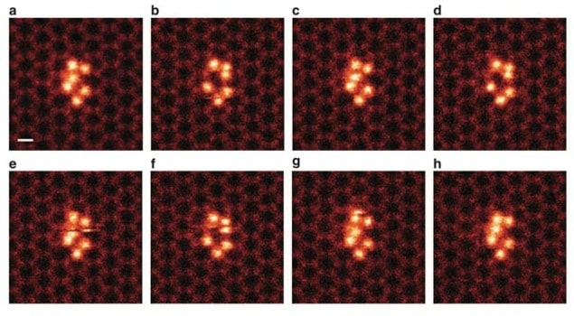
Researchers in the US have succeeded in directly visualizing the back-and-forth movement of silicon atoms that are clustered in graphene pores. Being able to analyse small clusters in this way could improve our understanding of how different atomic configurations determine a material’s properties. The ability to engineer clusters with specific properties could lead to new devices for electronics and optoelectronics. Also, a better understanding of how pores behave in graphene could lead to practical applications such as water desalination.
Working at the Oak Ridge National Lab (ORNL), the team achieved its feat by using graphene to trap groups of silicon clusters, each comprising six atoms. Graphene is a sheet of carbon just one atom thick that has a honeycomb lattice structure. The clusters were pinned in place by nanopores in the graphene, which allowed them to be directly imaged with a low-voltage (60 kV) aberration-corrected scanning transmission electron microscope (STEM).
Single-atom sensitivity
“The advantage of using an STEM compared with other microscopy techniques is that we can obtain crystallographic information about the sample – that is, atomic positions,” explains Oak Ridge’s Juan-Carlos Idrobo. “We can also chemically identify the elements present in the sample, either via imaging quantification or by spectrum imaging using electron energy loss spectroscopy (EELS). Another good advantage of STEM experiments is that they are sensitive to single atoms, something that has allowed us to directly count how many atoms were in the silicon cluster that we studied.”
This is not the first time that scientists have been able to look at clusters of silicon in the lab; but according to team member Jaekwang Lee, previous observations were indirect. Furthermore, it had not been possible to identify the exact 3D atomic structure of the clusters.
Not kicked out
One important observation made by the ORNL researchers is that one of the silicon atoms in the cluster changed its position within the structure, moving back and forth between two specific sites. “What was observed before in STEM imaging was that the atoms just get ‘kicked out’ of the sample by the high energy of the electron beam, but we spotted a silicon atom that stayed within the cluster and ‘danced’ around,” Idrobo says.
Using first-principles calculations, the team was also able to map the energies of the silicon cluster when it interacted with the electron beam and to calculate how much energy was required for an individual silicon atom within a cluster to switch back and forth between different positions.
“Capturing atomic clusters inside graphene nanopores may lead to applications in a range of areas, including electronics and optoelectronics, and catalysis,” adds Idrobo.
Studying catalysts
Looking to the future, one simple new experiment would be to pattern the graphene with pores of specific sizes and then embed clusters with different functionalities, Idrobo says. For example, clusters known to be catalytically active could be pinned in the graphene pores so that the researchers could directly study their atomic and electronic structures using the STEM.
The team is also looking at how the interaction between the clusters and the graphene could be used to develop graphene-based technologies. “Since silicon clusters are stable when embedded in graphene pores, we have decided to turn this finding on its head and are now investigating which elements are able to stabilize these pores,” explains Idrobo. “Stable pores with specific diameters could be used as very efficient molecular filters and might even be used in the future to desalinate water.”
The findings are detailed in Nature Communications.


