The ability to replicate the functionality of the human body is the ambitious aim of a lot of robotics research. However, with around 240 mechanical receptors per square centimetre in a human fingertip, reproducing the touch sensitivity of skin poses significant challenges. Wenzhuo Wu from Purdue University in the US told attendees of innoLAE 2018 how they had not just matched the number of receptors per square centimetre, but exceeded it by a factor of more than 20.
Zinc oxide nanowires have attracted a great deal of attention for their piezotronic properties, which modulates electronic transport directly by means of mechanical inputs. The fundamental principle of piezotronics was introduced by Zhong Lin Wang at Georgia Institute of Technology in 2007. The challenge for Wu and colleagues was to fabricate an array of individually addressable nanowire devices that might exploit this piezotronic response and collectively function as smart skin.
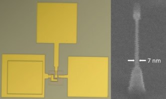
As well as drawing on his expertise in understanding and controlling the growth process to ensure well aligned nanowires and uniform height, Wu described how they also adopted a two-terminal device structure. “We remove the gate electrode,” said Wu, describing what they call a “piezotronic transistor”. Previously nanowire transistors have been fabricated using a wrap-around gate on each nanowire, however the piezotronic transistor has only two terminals. “It can be directly controlled by mechanical signals, so that these mechanical signals – like pressure and strain – function essentially as the gate controlling signal to modulate the transport,” adds Wu. “We think it is a powerful design especially for human machine interfacing.”
He and his colleagues in Wang’s team at Georgia Tech produced a device that can detect its own shape change using an array of these strain-gated vertical piezotronic transistors on a flexible polyethylene terephthalate (PET) substrate at a device density of 8464 devices per square centimetre – more than 20 times that of human finger tips. Wu also completed related work for tactile imaging during his PhD research in Wang’s group at Georgia Tech.
The researchers are now looking into how 2D material devices can function as strain-gated transistors. Other groups have looked at graphene, but Wu, in collaboration with his postdoc mentor Wang at Georgia Tech, has investigated single-atomic-layer MoS2, reporting on how the piezophototronic effect in the material may be used for strain-gated flexible optoelectronics back in 2016.
Speaking to nanotechweb.org after his presentation, Wu added, “I think currently there has been a huge amount of fantastic work exploring the fundamental science and concepts of all materials, but in order for the entire community to push it forward and make something impactful for society we must come up with an economic approach or platforms to integrate those nanomaterials holistically into designed structures as pre-designed.” He added, “You need to integrate them at large scale at very low cost so that you can truly make use of the new science and fundamental phenomenon, so manufacturing is I think the next big question.”
For more information on innoLAE and future conferences visit http://www-large-area-electronics.eng.cam.ac.uk/innoLAE2018.