Just when you thought that graphene could do no more, physicists in the US have found yet another new and unique property of the wonder material. The team has shown that when graphene – a sheet of carbon just one atom thick – is strained in a particular way, its electrons behave as though they are in strong magnetic field. The phenomenon, which had been predicted in theory, could be used to modify the electronic properties of graphene to make strain gauges or even transistors and optoelectronics components.
Since graphene was first created in 2004, its unique electronic and mechanical properties have amazed researchers, who have been eyeing up the material for a host of practical applications. In particular, it could be used to make ultrafast transistors because the electrons in graphene whizz through the material at extremely high speeds.
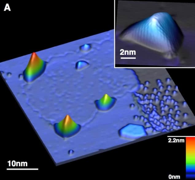
This latest property of graphene was discovered by Michael Crommie and colleagues at the University of California at Berkeley and the Lawrence Berkeley National Labs, who were trying to grow a graphene layer on the surface of a platinum crystal. It turns out that carbon atoms in graphene – which are organized in a hexagonal lattice – do not line up perfectly with the triangular crystal structure of the platinum. The resulting strain in the graphene causes tiny triangular structures to push out of the surface.
Moving in circles
These graphene “nanobubbles” are about 4–10 nm long and about 2 nm high. Because the structures are very small, the electrons within each nanobubble inhabit discrete energy levels. This is unlike electrons in unstrained graphene, which occupy continuous energy bands. These discrete energy levels, or “Landau levels”, are the same as those an electron would occupy if it were moving in circles in an extremely high magnetic field of around 300 Tesla.
The researchers observed the new electronic behaviour using a scanning tunnelling microscope (STM), which is able to determine the electron energy states in very small regions of the graphene’s surface.
A likely explanation for why the electrons orbit in circles, according to Crommie, lies in how the distance between the carbon atoms changes with applied strain. If graphene is strained in just the right way then these differences combine to cause an electron’s motion to bend just as if a magnetic field were present.
‘Pseudo-magnetic’ field
Further study of the effect could prove fruitful for two reasons, says Crommie. “First, it gives us a new way to explore the physics of electrons in graphene when they are subjected to high magnetic fields that could never be achieved in the laboratory,” he told physicsworld.com. Indeed, the “pseudo-magnetic” field experienced by the electrons is about 10 times bigger than the biggest steady state magnetic field ever achieved in a lab.
“Second, we can use the effect to modify the electronic properties of graphene by stretching it in certain ways,” he explains. This could lead to “straintronics” – devices with electronic properties that are engineered through the careful introduction of mechanical deformations in graphene. By using strain to control where the electrons gather – and the nature of their energy levels – devices with useful conductive, optical or microwave properties could be made.
“The effect could also be used to tune graphene’s structure in ways that could be useful for channelling graphene electrons into certain regions – to create dot and ribbon geometries for transport devices, for example”, he explains. “Now we know that such tuning is possible, it will be exciting to explore these different potential applications.”
‘Outside our wildest dreams’
Andre Geim of Manchester University in the UK, who discovered graphene back in 2004 and who was part of the team that recently predicted the very effect now observed by Crommie and colleagues, praises the new findings: “I never expected that our theoretical prediction would become relevant within only a few months and, moreover, in such a spectacular manner. We were hoping that by applying strain we could eventually generate fields of 10 Tesla or so. Although in agreement with the theory, 300 Tesla was outside our wildest dreams.”
Applying strain can do wonderful things to graphene’s electronic properties, he continued. “However, a number of further steps are needed before ‘straintronics’ becomes viable for applications.
“One such application could be using graphene as a strain sensor – an application that could be worth billions of dollars. Crommie’s team’s work puts sky-high limits on what really is possible for such sensors.”
The California team is now trying to better understand how it can control and tune the nanobubbles. “We want to find out what exactly electrons are doing in the nanobubbles and how they respond to different physical environments,” revealed Crommie.
The work is reported in Science 329 544.


