Researchers are working to improve the efficiency of multi-layer solar cells. Richard Stevenson explores whether their practical benefits are more likely to be realized in space than on Earth
For solar cells, efficiency really matters. This crucial metric determines how much energy can be harvested from rooftops and solar farms, with commercial solar panels made of silicon typically achieving an efficiency of 20%. For satellites, meanwhile, the efficiency defines the size and weight of the solar panels needed to power the spacecraft, which directly affects manufacturing and launch costs.
To make a really efficient device, it is tempting to pick a material that absorbs all the Sun’s radiation – from the high-energy rays in the ultraviolet, through to the visible, and out to the really long wavelengths in the infrared. That approach might lead you to build a cell out of a material like mercury telluride, which converts nearly all of the Sun’s incoming photons into current-generating electrons. But there is an enormous price to pay: each photon absorbed by this material only produces a tiny amount of energy, which means that the power generated by the device would be pitiful.
Hitting the sweet spot
A better tactic is to pick a semiconductor with an absorption profile that optimizes the trade-off between the energy generated by each captured photon and the fraction of sunlight absorbed by the cell. A material at this sweet spot is gallium arsenide (GaAs). Also used in smartphones to amplify radio-frequency signals and create laser-light for facial recognition, GaAs has long been one of the go-to materials for engineering high-efficiency solar cells. These cells are not perfect, however – even after minimizing material defects that degrade performance, the best solar cells made from GaAs still struggle to reach efficiencies beyond 25%.
Further gains come from stacking different semiconductors on top of one another, and carefully selecting a combination that efficiently harvests the Sun’s output. This well-trodden path has seen solar-cell efficiencies climb over several decades, along with the number of light-absorbing layers. Both hit a new high last year when a team from the National Renewable Energy Laboratory (NREL) in Golden, Colorado, unveiled a device with a record-breaking efficiency of 47.1% – tantalizingly close to the 50% milestone (Nature Energy 5 326). Until then, bragging rights had been held by structures with four absorbing layers, but the US researchers found that six is a “natural sweet spot”, according to team leader John Geisz.
Getting this far has not been easy, because it is far from trivial to create layered structures from different materials. High-efficiency solar cells are formed by epitaxy, a process in which material is grown on a crystalline substrate, one atomic layer at a time. Such epitaxial growth can produce the high-quality crystal structures needed for an efficient solar cell, but only if the atomic spacing of each material within the stack is very similar. This condition, known as lattice matching, restricts the palette of suitable materials: silicon cannot be used, for example, because it is not blessed with a family of alloys with similar atomic spacing.
Devices with multiple materials – referred to as multi-junction cells – have traditionally been based on GaAs, the record-breaking material for a single-junction device. A common architecture is a triple-junction cell comprising three compound semiconductors: a low-energy indium gallium arsenide (InGaAs) sub-cell, a medium-energy sub-cell of GaAs and a high-energy sub-cell of indium gallium phosphide (InGaP). In these multi-junction cells, current flows perpendicularly through all the absorbing layers, which are joined in series. With this electrical configuration, the thickness of every sub-cell must be chosen so that all generate exactly the same current – otherwise any excess flow of electrons would be wasted, reducing the overall efficiency.
Bending the rules
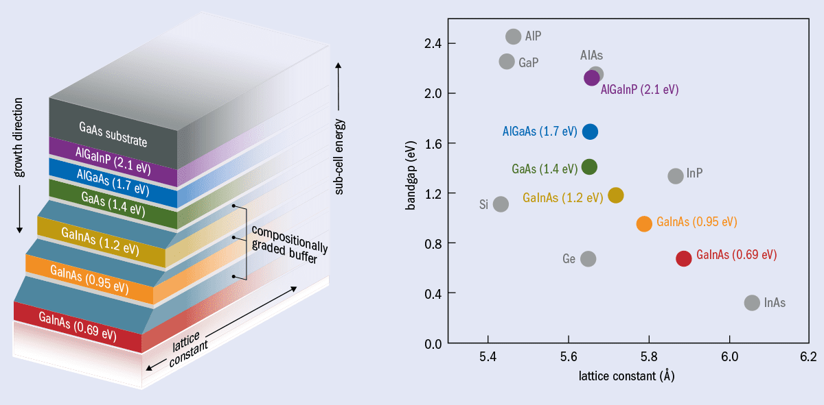
Key to the success of NREL’s device are three InGaAs sub-cells that excel at absorbing light in the infrared, which contains a significant proportion of the Sun’s radiation. Achieving strong absorption at these long wavelengths requires InGaAs compositions with a significantly different atomic spacing to that of the substrate. Additionally, their device has been designed with intermediate transparent layers made from InGaP or AlGaInAs to keep material imperfections in check. Grading the composition of these buffer layers enables a steady increase in lattice constant, thereby providing a strong foundation for local lattice-matched growth of sub-cells that are not riddled with strain-induced defects.
The NREL team, which has pioneered this approach, advocates the so-called “inverted variant” structure. With this architecture, the highest energy cell is grown first, followed by those of decreasing energy, so that the cells lattice-matched to the substrate precede the growth of graded layers. This approach improves the quality of the device, while the fabrication process also results in the removal of the substrate – a step that could trim costs by enabling the substrate to be reused.
One other technique that can further boost solar-cell efficiency is to focus sunlight on the cells, either with mirrors or lenses. The intensity of light on a solar cell is usually measured in “suns”, where one sun is roughly equivalent to 1 kW/m2. Concentrated sunlight increases the ratio of the current produced when the device is illuminated compared to when it is in the dark, thereby boosting the output voltage and increasing the efficiency. The gain is considerable: the NREL device achieves a maximum efficiency of just 39.2% when tweaked to optimize efficiency without any concentration, a long way short of the 47.1% record.
When Geisz and colleagues assessed how the performance of their six-junction cell varies with concentration, they found that peak efficiency occurs at 143 suns. Nevertheless, the device still produces a very impressive 44.9% efficiency at 1116 suns, which would generate a large amount of power from a very small device. As a comparison, a record-breaking cell operating at 500 suns could deliver the same power as a commercial solar panel from just one-thousandth of the chip area. At such high concentrations, however, steps must be taken to prevent the cell from overheating and diminishing performance.
Just over a decade ago, this approach to generating power from high-efficiency cells spawned a concentrating photovoltaic (CPV) industry, with a clutch of start-up firms producing systems that tracked the position of the Sun to maximize the energy that could be harvested from focusing sunlight on triple-junction cells. Unfortunately, this fledgling industry came up against the unforeseeable double whammy of a global financial crisis and a flooding of the market with incredibly cheap silicon panels produced by Chinese suppliers. The result was that so few CPV systems were deployed that even on a sunny day when all operate at their peak, their global output totals less than one-tenth of the power of a typical UK nuclear power station.
Extra-terrestrial encounters
Far greater commercial success for makers of multi-junction cells has come from powering satellites, most recently buoyed by the rollout of satellite broadband by companies such as OneWeb and Starlink. The key advantage here is that high-efficiency cells can drive down the costs of making and launching each satellite. As well as reducing the number of cells needed to power the spacecraft, higher efficiencies shrink both the size and weight of the solar panels that form the “wings” of the satellite. While launch costs have plummeted over the last few decades, satellite operators can still expect to pay almost $3000 per kilogram to get their spacecraft into orbit – and thousands of satellites are due to be deployed over the next few years.
For a solar cell in space, the crucial metric is the value at the end of its lifetime – after the device has been bombarded by radiation
However, for a solar cell in space, the crucial metric is not the initial efficiency but the value at the end of its intended lifetime after the device has been bombarded by radiation. Compound semiconductors hold up to this battering far better than those made from silicon. Early studies showed that the difference in efficiency of compound semiconductors rises with age from 25% to 40–60%, which ensured the dominance of triple-junction cells for space applications. Even so, the efficiencies of the best commercial cells for satellites remain limited to around 30–33%. This is partly because the solar spectrum beyond our atmosphere has a stronger contribution in the ultraviolet, where it is much harder to make an efficient cell, and partly because there are no concentrating optics to focus sunlight onto the cell.
To drive down the watts-per-kilogram of solar power in space, a US team working on a project known as MOSAIC (micro-scale optimized solar-cell arrays with integrated concentration) has been making a compelling case for CPV in space. The team points out that it should be relatively easy to orientate the solar panels on a satellite to maximize power generation with lenses in front of the cells shielding them from radiation. Concentrations must be limited to no more than around 100 suns, however, because cells in space cannot be cooled by convection, only by heat dissipation through radiation and conduction.
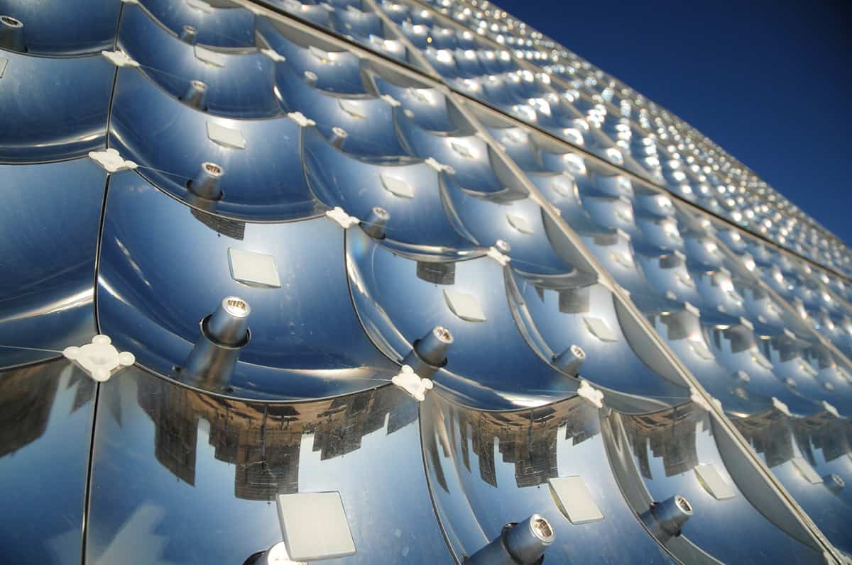
For CPV to have a chance of succeeding in space, the large and heavy solar modules used in early terrestrial systems must be replaced with a significantly slimmed-down successor. Technology pioneered by project partner Semprius, a now defunct CPV system maker, excels in this regard. The firm developed a process that uses a rubber stamp to parallel-print vast arrays of tiny cells, each one subsequently capped by a small lens.
The best results have come from stacking a dual-junction GaAs-based cell on top of an InP-based triple-junction cell separated by a very thin dielectric polymer. Current cannot pass through this polymer film, so separate electrical connections are made to extract the current from each cell independently. While this doubles the number of electrical connections, it eliminates the need for current matching between the two devices. Lifting this restriction gives greater freedom to the design, potentially enabling this approach to challenge the efficiency of NREL’s record-breaking device under high concentrations. Operating at 92 suns under illumination which mimics that in space, the team’s latest device, still to be fully optimized, has an efficiency of 35.5%.
Towards 50%
The NREL researchers know what they need to do to break the 50% barrier. The goal they are chasing is to cut the resistance in their device by a factor of 10 to a value similar to that found in their three- and four-junction cousins. They are also well aware of the need to bring down the cost of producing such complex multi-junction cells.
Also chasing the 50% efficiency milestone is a team led by Mircea Guina from Tampere University of Technology in Finland. Guina and colleagues are pursuing lattice-matched designs with up to eight junctions, including as many as four from an exotic material system known as dilute nitrides – a combination of the traditional mix of indium, gallium, arsenic and antimonide, plus a few per cent of nitrogen.
Dilute nitrides are notoriously difficult to grow. Back in the 1990s, German electronics powerhouse Infineon developed lasers based on this material, but they were never a commercial success. More recently, Stanford University spin-off Solar Junction showcased the potential of this material in solar cells. Although the start-up went to the wall when CPV flopped, devices produced by the company grabbed the record for solar efficiency in 2011 and raised it again in 2012 with triple-junction designs. Guina and co-workers are well positioned to take their technology further. They have made progress in producing all four of the dilute nitride sub-cells needed to produce record-breaking devices, and their efforts are now focused on optimizing the high-energy junction. The team’s work has been delayed due to the COVID-19 pandemic, but Guina believes that the approach could break the 50% barrier, possibly raising the bar as high as 54%.
There is still a question of impetus, however. The lack of commercial interest in terrestrial CPV may well encourage Guina to change direction and focus on chasing the record for space cells with no concentration. Much of today’s multi-junction solar-cell research is not focusing on power generation here on Earth, so while that 50% milestone is tantalizingly close, it might not be broken anytime soon.

