Researchers in Taiwan and the US have developed a technique that could lead to the large-scale production of optical “metamaterials”. The team used the technique, which is based on a well-established deposition method, to fabricate thin films of silver nanorods on a silicon substrate. The resulting composite material can manipulate light in unusual ways and could enable a range of applications in the photonics industry, say the researchers.
“Our technique should couple naturally with much of microelectronics” Akhlesh Lakhtakia, Pennsylvania State University
Metamaterials are materials that have been artificially engineered to have unusual electromagnetic properties. They have generated a lot of interest in the last few years, largely because they could produce exotic applications like invisibility cloaks and “superlenses” – that have higher resolution than traditional correction lenses. Unfortunately, the metamaterials made so far have only worked over a limited range of frequencies and are difficult to produce in large quantities.
Taking a different approach, Yi-Jun Jen of Taipei University of Technology, Taiwan, and his colleagues, have turned their attention to a more established production technique known as “oblique angle deposition” (OAD) which is widely used in the photonics industry to deposit thin films. It involves depositing vapour at an angle onto a substrate held in a vacuum.
Emerging from the shadows
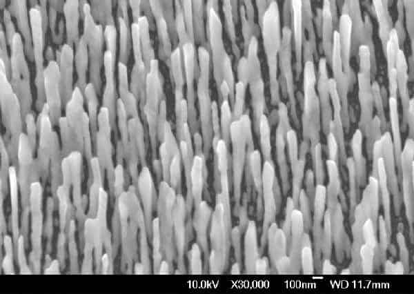
Jen and his colleagues first vaporized a block of silver by firing electrons into it and then directed the vapor at two-inch substrates of silica material. Deposits tend to accumulate in patches on the substrate but — at certain angles to the substrate norm — nanorods can grow preferentially towards the incoming vapor because of the “self-shadowing effect”.
The film thickness was 240 nm and the angle between the normal to the substrate and the tilt of the nanorods was maintained at 66 degrees. Silver nanorods were grown to about 650 nm long and 80 nm wide.
The researchers then determined the optical properties of the film by illuminating it a number of times with light at wavelengths between 300 and 850 nm. They found that light between the wavelengths 532nm and 690 nm was refracted negatively but say that – in theory – almost all visible light (380 to 750 nm) could be negatively refracted (arXiv 0903.1177v1 ).
Simple is best
“Of course, such films had been grown by others but no one thought to characterize them as biaxial dielectric-magnetic materials,” said Akhlesh Lakhtakia , one of the researchers, at Pennsylvania State University.
“Their results are interesting because of the simplicity on the fabrication of the layers of nanorods,” said Jaime Gomez Rivas of the Nanowire Photonics group at the AMOLF Institute in Eindhoven.
Lakhtakia told physicsworld.com that the next step is to explore the effect of morphology and start developing layered structures to avoid energy attenuation.
“Since OAD technology is a planar technology, this production method should couple naturally with much of microelectronics,” he added.


