
While theories abound to explain the lag between investment and commercial return in graphene research, a supply chain flooded with samples of graphite masquerading as graphene certainly won’t help. Yet when researchers at the National University of Singapore systematically analysed samples from over 60 suppliers based in America, Asia and Europe, they found most contained less 10% of what the International Standardization Organization defines as graphene, with just one sample containing more than 40% high-quality graphene, as reported in Advanced Materials.
“It is alarming to uncover that producers are labelling black powders as graphene and selling them for top dollar, while in reality, they contain mostly cheap graphite,” says Antonio Castro Neto, Director of the NUS Centre for Advanced 2D Materials, who led the study. “There is a strong need to set up stringent standards for graphene characterization and production to create a healthy and reliable graphene market worldwide.”
Suffering from a few too many
The miraculous properties of graphene have attracted headlines ever since the material was isolated and characterized by Kostya Novoselov and Andre Geim, who were awarded a Nobel Prize for the work in 2010. Strictly speaking graphene is a single layer of carbon atoms arranged in a honeycomb like lattice, but “few-layer” graphene can retain much of the fascinating alliance of extraordinary electrical and mechanical properties. However when the number of layers starts to number more than just a few, the wonder material behaves less and less like graphene and more and more like graphite, also known as pencil lead.
Graphene service provides missing link for industry
The importance of distinguishing graphene from graphite has been recognized for several years, prompting the International Standardization Organization to set a precise definition for what can be defined as graphene – fewer than 10 layers. While this clarifies things for patent attorneys, a definition is little use to the graphene sector if suppliers continue to supply graphite in place of graphene, and users lack the resources to distinguish graphene flakes from graphene fakes.
“Whether producers of the counterfeit graphene are aware of the poor quality is unclear,” says Neto. “Regardless, the lack of standards for graphene production gives rise to bad quality of the material sold in the open market. This has been stalling the development of the future applications.”
The results of the NUS study come just months after the establishment of the Graphene Service in the UK, a collaboration between the National Physical Laboratory in Teddington and the National Graphene Institute at the University of Manchester. The Graphene Service aims to leverage the expertise in the two institutions to characterize samples for users and provide advice on their potential uses.

Evaluating foundry solutions
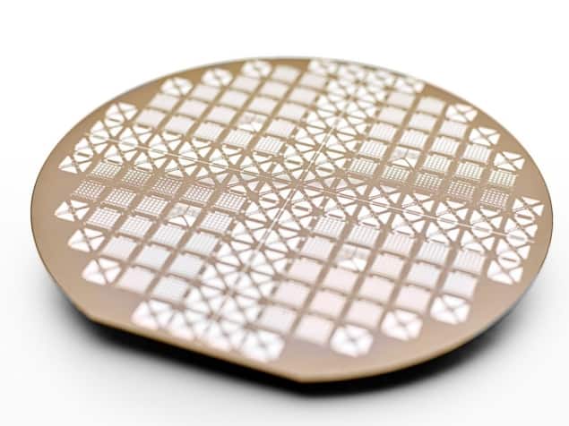
In Europe investment in graphene to the tune of €1 billion in the form of the Graphene Flagship has set an unprecedented high bar on expectations for the material’s worth. While little research is possible without funding, funding alone is little guarantee of commercially successful research, and the difficulty of the task should not be ignored when questioning the time taken to cash in on graphene research investments. With a view to easing at least one stage of the process, Graphene Flagship partner Graphenea have now released the Graphene Foundry service, aimed at “enabling fast device prototyping and accelerating development of new applications, lowering entry barriers to graphene-based solutions.”
The foundry offers to manufacture custom circuit designs on graphene wafers up to 6” and promises stringent quality control on all of its samples using Raman spectroscopy, optical microscopy and electrical tests. While you can bag a Grapehenea field effect transistor device at $385, a 4” wafer could set you back $7,950.00. Given the value placed on the graphene market once its true potential is unleashed, some might say an option that side-steps the pencil peddlers and other fabrication pitfalls would be cheap at twice the price.


