Researchers at East China Normal University in Shanghai have found the first evidence for electronic band gap closing in a family of layered materials known as three-dimensional topological insulators. The researchers obtained this result thanks to a molecular beam epitaxy technique that allowed them to orient the material’s layers as they grew. The work could aid the development of more energy-efficient electronic devices made from these materials and might also open a new route to search for possible exotic states in these systems.
Within the past few years, physicists and materials scientists have developed ways to manipulate the electronic properties of two-dimensional materials by twisting their atomically-thin layers with respect to each other. This technique, dubbed “twistronics”, was first demonstrated in graphene (a 2D sheet of carbon) and has since been extended to 3D materials such as the topological insulators in the Shanghai team’s work.
Like graphene, 3D topological insulators can host unusual band structures known as “Dirac cones” that allow charge carriers to behave like 2D massless Dirac particles – meaning that they can travel through a material at very high speeds. Such high charge mobilities mean that transistors and other electronics devices based on these novel materials could be faster and more energy efficient than those made from conventional materials.
In topological insulators, Dirac cones occur on the material’s surface in special “topologically protected” electronic states known as quantum spin Hall (QSH) states. These QSH states can “hybridize” and open up a band gap, transforming the initially insulating materials into electrical conductors. This band gap is predicted to close up again, but such a topological “phase transition” had never previously been observed experimentally.
Multilayer twists
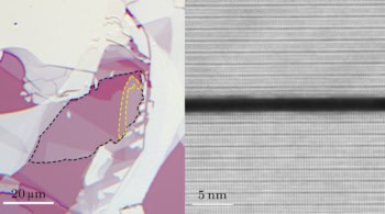
In their work, Yeping Jiang and colleagues studied ultra-thin samples of antimony telluride (Sb2Te3). This compound is composed of stacks of quintuple layers held together by weak van der Waals interactions. It can be cleaved into few-layer or even monolayer films that, like graphene, can then be stacked together in a controllable way to make twisted structures. In the case of monolayers, 2D massless Dirac electrons appear on the top and bottom surfaces of the layers.
The researchers used a molecular beam epitaxy technique to grow Sb2Te3 structures containing three such layers. The good thing about the technique is that it allows them to twist the angles between the layers in situ – that is, during growth.
Nanostructured topological insulator growth speeds up
Thanks to scanning tunnelling spectroscopy measurements, they found that their film had an intrinsic hybridization gap of 60 meV, which is small enough to allow a topological phase transition of the type they were looking for. They also observed signatures of electron band gap closing for some twist angles. Their future work, they say, will focus on the gap-closing regime to obtain more solid evidence for this phase transition.
“To the best of our knowledge, ours is the first experiment to realize twisted structures of topological insulators using an in situ technique, Jiang tells Physics World. “Our work will hopefully allow us search for possible exotic states in these systems.”
The researchers report their work in Chinese Physics Letters.