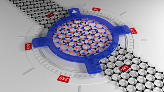
Researchers at Columbia University in the US have developed a new device structure in which they can vary the “twist” angle between layers of 2D materials (such as graphene) and study how this angle affects their electronic, optical and mechanical properties. The measurements, which are carried out on a single structure rather than multiple ones (as was the case before), could advance the emerging field of “twistronics” – a fundamentally new approach to device engineering.
“In recent years, researchers have realized that the weak coupling between different layers of 2D materials can be used to manipulate these materials in ways that are not possible with more conventional structures,” explains Cory Dean, who led this research effort together with James Hone. “One dramatic example is being able to modify their electronic properties by varying the angle between the layers.
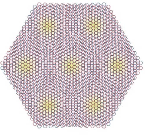
“For instance, graphene (a 2D sheet of carbon atoms) normally does not have a band gap. It develops one, however, when placed in contact with another 2D material, hexagonal boron nitride, which has a closely matching lattice constant. The layers of graphene and boron nitride form what is called a large “Moiré superlattice”. By then twisting the layers so that they become misaligned and the angle between them becomes large, the band gap disappears.

“Simply varying the angle between 2D material layers thus means that graphene can be tuned from being metallic to semiconducting. Indeed, researchers at the Massachusetts Institute of Technology (MIT) recently discovered that placing two layers of graphene together, but rotated relative to one another at the ‘magic’ angle of 1.1° turns the normally metallic material into a superconductor.”
Achieving this variety of electronic properties in conventional materials normally requires changing their chemical composition. The ability to vary the electronic property of a 2D material simply by altering the twist angle between its layers is therefore a fundamentally new direction in device engineering, he adds.
Single device
Until now, researchers needed to make a whole new device for each different twist angle. This often involved fabricating a large number of devices, which also made it difficult to resolve angle-dependent effects independent of sample-to-sample variations.
“What is more, many of the interesting angle-dependent characteristics (such as the above-mentioned superconductivity in twisted bilayer graphene), could only be observed within a very narrow range of the target angle,” says Dean. “We have now succeeded in making a single device whose layers we can continuously rotate locally while measuring its physical and electronic properties. This is a new platform that allows us to switch between an arbitrary number of complementary states in the device.”
So how did the Columbia team do this? “Our technique takes advantage of the low interfacial friction that naturally exists between layered 2D materials,” Dean tells Physics World. “There is no strong chemical binding between the layers so they slide over one another easily. Indeed, this is the reason that graphite is used in pencil lead and that both graphite and boron nitride are used as dry lubricants in industry.”
In their fabrication process, the Columbia researchers studied graphene/boron nitride heterostructures and designed a device in the shape of a gear that they intentionally made so that it was rotatable. “We then employed techniques previously developed in our lab to mechanically pick up this nano-sized gear (made of boron nitride) and place it over the top of the active area (graphene). Once in place, we used an atomic force microscope to push along one tooth of the gear, causing it to rotate.”
Proof-of-principle
This proof-of-principle shows that we can achieve and control rotation in graphene/boron nitride heterostructures, and can dynamically vary the electrical, optical and even mechanical properties of a device made from these structures, he says.
“Notably, we demonstrated that the energy gap observed in graphene is tuneable and can be turned on or off on demand just by changing the orientation between the layers,” adds Rebeca Ribeiro, who is lead author of the study.
As for applications, the work could help in the development of new kinds of switching technologies, such as tuneable sensors and tuneable electro-mechanical and electro-optical based devices, says Dean.
The researchers, reporting their work in Science 10.1126/science.aat6981, say that they are now busy studying emerging phenomena that come from interactions between the 2D material layers. “The discovery of superconductivity in twisted bilayer graphene results from the interaction between single layers of graphene, neither of which superconduct on their own. We believe that we might be able to introduce, and turn on and off, similar effects, such a spontaneous magnetic ordering and topologically protected band gaps, with controlled twisting.
‘Magic-angle graphene’ behaves like a high-temperature superconductor
“Until now, we have only studied graphene and boron nitride but there exists a large class of 2D materials that can be integrated with one another in similar ways. These materials can be metallic, insulating, semiconducting, magnetic and superconducting.
“At the most basic level, our study shows that there is a fundamentally new way to control these materials that just doesn’t exist in conventional semiconductor heterostructures. It therefore opens the door to a whole new field of research in which material properties can be varied by simply twisting material layers.”


