Bespoke vacuum sample environments at synchrotron X-ray facilities reveal nanoscale kinetics, chemical transformations and other processes relevant to materials synthesis, explains Paul Evans

It is 100 years since father-and-son team William and Lawrence Bragg won the Nobel Prize for Physics for their discovery of X-ray crystallography. This powerful technique exploits the fact that X-rays produce a characteristic diffraction pattern when they pass through a crystalline sample. From these patterns researchers can infer the atomic structure of matter – ranging from new materials to biological molecules.
Pioneering crystallographers relied on low-intensity X-ray sources similar to those found in hospitals to determine the structure of simple crystals such as salt and, later, the famous double helix of DNA. Since the 1980s, however, researchers have had much more powerful synchrotron X-ray light sources at their disposal. These enable studies not only of the basic crystalline structure of materials, but also their assembly, interfaces, defects and transformations. More than 30 major synchrotron light sources are currently in operation worldwide and are used by tens of thousands of researchers each year, spanning numerous scientific disciplines.
The extremely high brightness and excellent stability of synchrotron radiation, combined with optical elements that can focus X-ray beams to spot sizes just tens of nanometres across, allow researchers to probe isolated nanostructures or interrogate small volumes within complicated heterogeneous systems such as semiconductor devices. The creation of coherent X-ray beams with well-defined wavefronts is a crucial aspect of the technique, and recent advances in coherent X-ray scattering with smaller spot sizes are providing new insight into nanoscale materials.
Serious challenges
Applying these emerging X-ray techniques in controlled sample environments – particularly at elevated temperatures under vacuum or controlled gas environments – provides even deeper insight into processes relevant to materials synthesis. It allows researchers to study critical processes, such as the atom-by-atom growth of thin films for electronic and optics devices, under conditions relevant to manufacturing processes. The technique also allows users to study a material’s intermediate structures, which could be unstable at room temperature or under atmospheric pressure. Without isolating samples under controlled vacuum environments it is impossible to probe these subtle physical and chemical processes, but the use of X-ray nanobeams also presents serious challenges for vacuum technology.
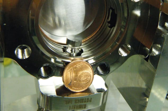
Applying X-ray nanobeam techniques in non-ambient conditions is hindered mainly by mechanical constraints. Nanobeam diffraction requires creating instruments that are very robust against displacements caused by ambient acoustic or mechanical noise and also robust against angular instabilities. The relative displacement between the sample and focusing optics must be much less than the beam size (typically 100 nm today), while the sample’s orientation must be stable to within 1 mdeg. The latter is equivalent to the angle subtended by a penny observed at a distance of 1 km.
Nanobeam diffraction requires creating instruments that are very robust against displacements caused by ambient acoustic or mechanical noise and also against angular instabilities
X-ray diffraction experiments also involve repeated measurements in the same small region of the sample, which requires the position of optical elements to be stable to within a few microns per hour. Finally, the short-wave nature of X-rays compared with visible light means that the working distances of X-ray optics are comparatively large, such that the focusing optics can be placed up to a few centimetres away from the sample. Even so, that means squeezing the vacuum environment into a space far smaller than the typically 0.5–1 m diameter of traditional vacuum chambers used for materials research.
Integrated sample environments
Researchers from the University of Wisconsin in the US and the European Synchrotron Radiation Facility (ESRF) in Grenoble, France, have recently developed a new approach with which to integrate precise vacuum sample environments with X-ray nanobeam experiments. The result is a series of high- and ultrahigh-vacuum (UHV) sample environments that are compact and light enough to be integrated with nanopositioners and X-ray nanobeam optics at modern synchrotrons.

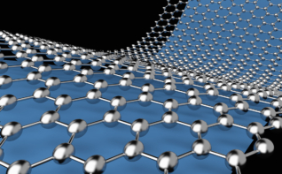
The initial device – a UHV environment – was integrated with a hexapod nanopositioner that enabled the collection of maps and diffraction patterns without degrading resolution or precision. The set‑up contains small sputter-ion vacuum pumps that have no moving parts and thus exhibit reduced vibrations and better positional and orientation stability compared with turbomolecular pumps. The UHV environment is maintained in a stainless-steel chamber with metal seals and welded thin beryllium windows, and the device weighs just 1.4 kg. A series of demonstration experiments probed the motion of gold atoms on a silicon surface, resulting in the formation of large, 100 nm-scale gold crystals (Rev. Sci. Instrum. 84 113903). Similar processes of atomic transport on surfaces are relevant for developing next-generation semiconductors such as 2D chalcogenides and graphene.
A true UHV environment, however, is not required for all experiments and in many cases a high-vacuum environment is sufficient. Examples include aging processes of devices for which the critical parts are often not exposed at the surface, and thin-film phase transitions for which sub-monolayer-scale control of the surface composition is not required. The team at the ESRF’s ID01 beamline has thus subsequently developed a compact aluminum high-vacuum chamber evacuated with a turbomolecular pump and equipped with dome-shaped X-ray windows made either from beryllium metal or from polymers. Requiring only high vacuum reduces the mass of the system further, allowing users to combine the cell with piezoelectric positioners that allow samples to be moved with high precision.
Scanning X-ray diffraction microscopy at elevated temperatures in vacuum under diffraction conditions has become an important method of investigation for materials research and condensed-matter physics at ESRF’s dedicated X-ray nanodiffraction beamline. For example, the ESRF team’s high-vacuum environment has recently been used to study interfacial processes that can distort silicon’s crystal lattice (Appl. Phys. Lett. 106 141905). Integrating silicon with an ever-increasing spectrum of materials has been instrumental in advancing integrated-circuit technology. The combination of vacuum environments and X-ray nanobeam techniques allows the chemical reactions and atomic motion that determine the properties of these interfaces to be studied at the small length scales relevant to devices.
Fast-paced expansion
The next several years will see an increasingly fast pace of development of X-ray light sources, with orders-of-magnitude improvements in brightness provided by new synchrotrons under construction. Experimental facilities based in the target areas of these sources will vastly extend the application of X-ray nanobeams and expand the scientific community employing these techniques. The creation of vacuum environments with even lower mass and greater stability has an important role in enabling the materials-research community to apply these advances to challenging nanoscale structural phenomena.


