Welcome to the latest in a new series of sponsored articles showcasing some of the latest white papers from physics-based businesses around the world
This time we are featuring white papers from WITec, Ocean Insight, and Photonic Science and Engineering.
Studying semiconductors
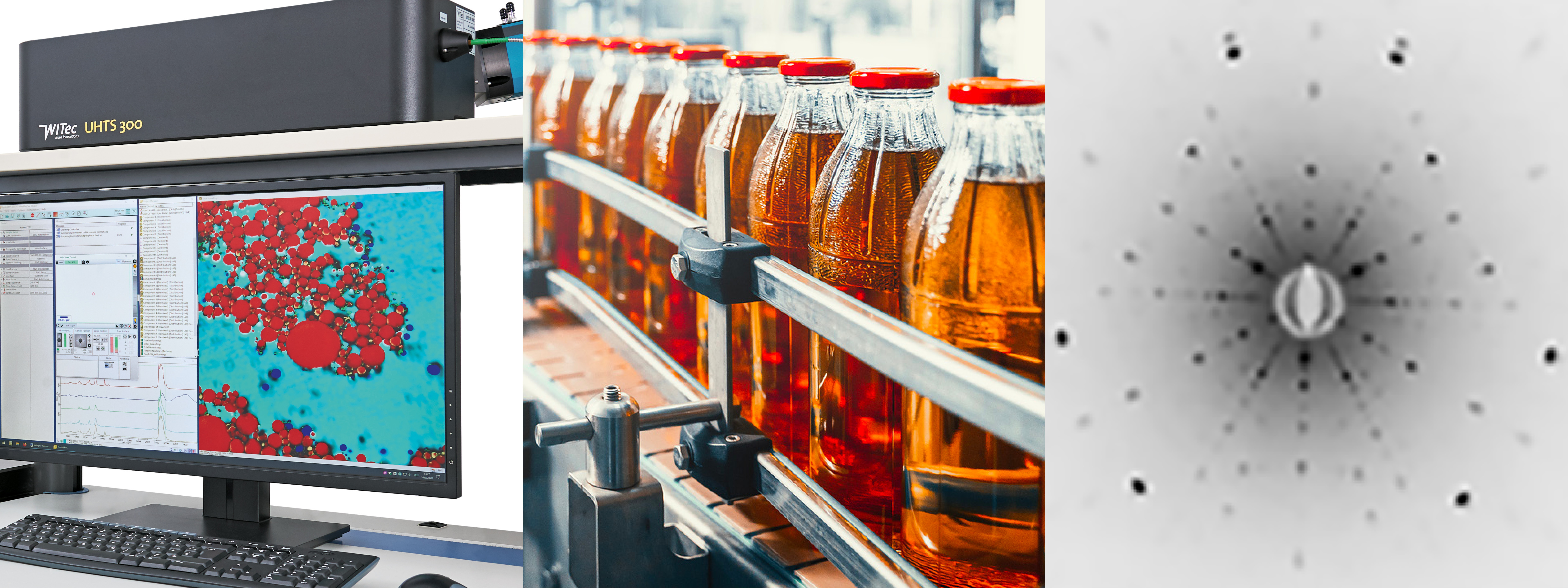
Raman spectroscopy is a long-established, non-destructive technique for studying solids, liquids and gases that involves measuring how light scatters inelastically off the component molecules. In Correlative Raman Imaging of Semiconducting Materials – the latest application note from WITec – you can find out how confocal Raman microscopy, which combines Raman spectroscopy with confocal microscopy, is a great way for characterizing semiconducting materials. The document shows how it can reveal the chemical composition of a sample, identify possible contaminants and even visualize strain fields in 3D volumes. Confocal Raman microscopy can even be combined with atomic-force microscopy or scanning-electron microscopy to allow semiconductors to be comprehensively investigated.
Innovative insights
![]()
Navigating today’s industrial landscape is an ongoing challenge for manufacturers, with dynamic regulatory issues, emerging technologies and global competition placing a premium on innovation and creativity. Manufacturers are therefore constantly looking for better ways to manage their supply chains, reduce waste and off-specification product, and increase production yields, which is where spectrometers, cameras and multispectral sensors come in. In its latest white paper Unlocking the Unknowns of Industrial Sensing, Ocean Insight shows how it offers robust, scalable sensing tools to help users unlock the unknowns of industrial applications especially in industrial sensing – from measuring colour and spotting defects to testing samples and sorting and grading products. Machine learning and custom algorithm development capabilities add another layer of insight, the paper adds.
Cleverly orientated

Laue diffraction is a powerful method for investigating crystal orientation. UK firm Photonic Science and Engineering has now developed a special Laue tool that fires an intense, polychromatic “white” beam onto a single crystal material positioned behind a very-low-noise CMOS detector. A back-reflection geometry records as many Bragg reflections as possible within a single exposure, delivering a “misorientation” value against the primary reference axis. In Laue Crystal Orientation System used in Micro-Diffraction Experiment you can find out how this technique has been used at the European Synchrotron Radiation Facility in Grenoble, France, and elsewhere, to study semiconductor detectors, sapphire substrates, laser or gamma scintillation materials, ceramics and metal alloys.