Researchers in the US have succeeded in removing single layers of atoms from graphene for the first time. The technique will be crucial for fabricating high-performance electronic devices from the “wonder material”.
Graphene is a sheet of carbon just one atom thick and is a promising material for making extremely small electronic devices of the future. This is thanks to its unique electronic and mechanical properties that include extremely high electrical conductivity and exceptional strength. However, it is difficult to separate the individual layers of graphene from each other because they tend to stick together. Although ordinary sticky tape can be used to strip off several layers at a time, there is still no reliable way to peel off exactly one layer and certainly not in specific patterns for microelectronic device fabrication.
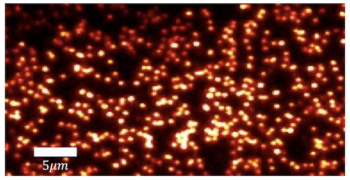
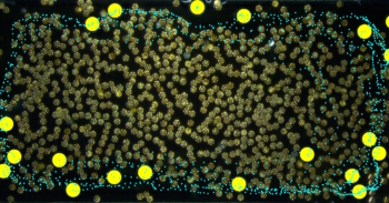
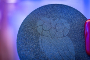
Now, James Tour and colleagues at Rice University may have overcome this problem by sputtering (or coating) selected areas of the top-most graphene layer in a sample with zinc and then applying hydrochloric acid to the surface as a wash. The technique removes the coated areas of graphene while leaving the uncoated areas and the layers below intact. The process can be repeated to produce multiple patterned layers, say the researchers, or even “chequerboard” structures by removing horizontal and vertical layers to create 3D patterns.
Highest precision lithography ever
“Being able to remove one layer at a time from graphene is the highest precision lithography that has ever been attained, or could ever be attained, for this – or indeed any other material – since it is made of single atoms layers,” Tour told physicsworld.com. The technique not only works for graphene, but also for graphene oxide.
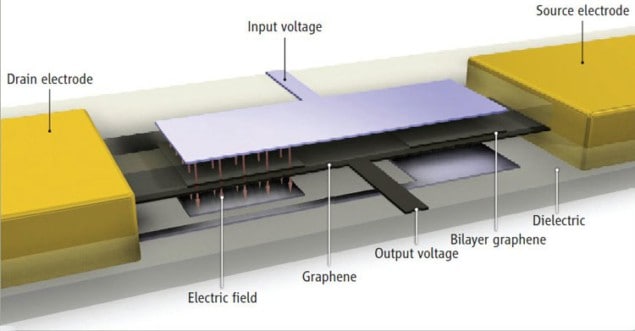
The method can also be used on thick films of graphene to selectively thin them down and pattern them into device structures. For example, a device such as an inverter could be made by depositing a bilayer of graphene onto pre-defined electrodes made of a metal and then peeling away some areas so that only monolayers remain here (see figure). The researchers confirmed that they had indeed removed single layers of graphene by imaging the samples in a scanning electron microscope and measuring the thicknesses of the remaining layers by atomic force microscopy.
Although they are not sure of the exact mechanism by which graphene layers peel, the researchers reckon that the zinc seems to damage the layers it coats by creating defects in the graphene. These damaged layers are then more easily removed by the subsequent acid wash step. Indeed, Raman spectra of the sputter-coated samples are characteristic of amorphous carbon, which suggests that the original crystalline structure of the graphene has been severely disrupted.
Encouraged by these new results, the team would now like to optimize its technique and control horizontal patterning of graphene layers with the same precision that has been achieved in the vertical direction. It also hopes to be able to better remove contaminants introduced during the sputtering process.
The results are detailed in Science.


