Ultrafast detector spies on multiple electrons in quantum dots
New device could lead to more efficient solar cells
 Read article: Ultrafast detector spies on multiple electrons in quantum dots
New device could lead to more efficient solar cells
Read article: Ultrafast detector spies on multiple electrons in quantum dots
The venerable "journal club" concept is thriving in the online environment
 Read article: Web life: Journal Club for Condensed Matter Physics
Japanese art of paper cutting used to make micron-sized electronic and mechanical devices
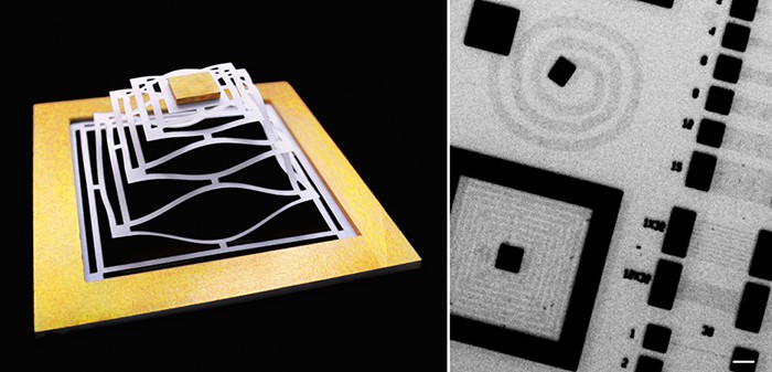 Read article: Stretchable graphene transistors inspired by kirigami
A biography of Silicon Valley's "quiet revolutionary", Gordon Moore, gets Paul Michael Grant thinking about the future of Moore's eponymous law
 Read article: Room at the bottom
Silicon-germanium and extreme ultraviolet lithography keep Moore's law on track
 Read article: Computer-chip features shrink to 7 nm
Research could help build photonic devices from novel 2D transition metals
 Read article: Thin semiconductors go through the Mott transition
Devices could be used to make transparent, flexible displays of the future
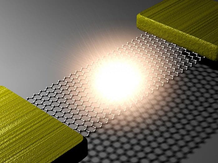 Read article: Graphene light bulb shines bright
New English-language translation of original 1959 paper

Silicon-based device would boost optical bandwidth
 Read article: Infrared detector to free up Internet of tomorrow
Magnetic measurement could boost the fortunes of spintronics
 Read article: Spin currents endure at room temperature in germanium
