Gigantic X-ray “tsunami” spotted near galaxy cluster
A giant wave of hot gas twice the size of the Milky Way has been discovered using NASA’s Chandra X-ray Observatory, radio observations and computer simulations. The wave is located near the Perseus galaxy cluster – one of the most massive nearby groupings of galaxies that spans 11 million light-years. It is the brightest cluster in terms of X-ray emissions because most of its observable matter is a gas that is so hot (tens of millions of degrees) it only glows with X-rays. Chandra has observed a variety of features in the gas, including a concave “bay” wave. If this structure was a result of bubbles launched by the central galaxy’s supermassive black hole, it would emit radio waves. However, observations by the Karl G Jansky Very Large Array in the US showed no such signal. It also could not be the result of “sloshing” gas as it arcs in the wrong direction. To work out the wave’s origin, Stephen Walker from NASA’s Goddard Space Flight Center in the US and colleagues compared high-resolution observational data with computer simulations of merging galaxy clusters. The resulting simulation begins with a large galaxy cluster (Perseus) that has settled into a “cold” (30 million degrees) central region surrounded by a zone of gas three times hotter. A small galaxy cluster then skirts the larger relative, causing a gravitational disturbance that churns up the gas and creates an expanding spiral of cold gas. Roughly 2.5 billion years later, the gas has spread 500,000 light-years from the centre and massive waves, such as the bay, form and roll at its periphery for hundreds of millions of years before dissipating. In the Monthly Notices of the Royal Astronomical Society, the scientists suggest that the waves are giant Kelvin–Helmholtz waves – which occur when there is a velocity difference at the interface of two fluids, such as wind blowing over water.
First light for European X-ray Free Electron Laser
Light at the end of the tunnel: the European XFEL. (Courtesy: DESY)
The European X-ray Free Electron Laser (European XFEL) in Hamburg, Germany, has achieved first light. Last month, engineers at the facility sent electrons down the facility’s 2.1 km-long superconducting linear accelerator for the first time. After being accelerated, electrons have now been sent through “undulators” to produce X-rays with a repetition rate of one pulse per second. When fully commissioned, the European XFEL will generate pulses of X-rays 27,000 times per second with each pulse lasting less than 100 fs (10–13 s). This will allow researchers to create “movies” of processes such as chemical bonding and vibrational energy flow across materials. Engineers will now continue commissioning the European XFEL – including increasing the facility’s repetition rate – ready for first users in September.
Survey highlights UK–Europe science collaboration
Scientists in the UK have strong collaborations with their European counterparts, according to a survey carried out by the UK National Academies. The Academy of Medical Sciences, British Academy, Royal Academy of Engineering and the Royal Society asked more than 1286 fellows and grant recipients about their international collaborations and mobility. They found that 95% had travelled to Europe and 87% collaborated with their European colleagues, while 58% of respondents had spent a year or more working abroad, 64% of whom went to North America. Meanwhile, a separate survey carried out by the Royal Society of 1285 UK-based scientists found that 72% had trained or worked abroad, while 80% of non-UK national researchers that were working in the UK were from the European Union or North America. The Royal Society survey also reported that women are less likely to work abroad than men. Some 39% of men say they had spent more than three years working outside of the UK compared to 25% for women.
You can find all our daily Flash Physics posts in the website’s news section, as well as on Twitter and Facebook using #FlashPhysics.
A photonic chip that allows a conventional microscope to work at nanoscale resolution has been developed by a team of physicists in Germany and Norway. The researchers claim that as well as opening up nanoscopy to many more people, the mass-producible optical chip also offers a much larger field of view than current nanoscopy techniques, which rely on complex microscopes.
Nanoscopy, which is also known as super-resolution microscopy, allows scientists to see features smaller than the diffraction limit – about half the wavelength of visible light. It can be used to produce images with resolutions as high as 20–30 nm – approximately 10 times better than a normal microscope. Such techniques have important implications for biological and medical research, with the potential to provide new insights into disease and improve medical diagnostics.
“The resolution of the standard optical microscope is basically limited by the diffraction barrier of light, which restricts the resolution to 200–300 nm for visible light,” explains Mark Schüttpelz, a physicist at Bielefeld University in Germany. “But many structures, especially biological structures like compartments of cells, are well below the diffraction limit. Here, super-resolution will open up new insights into cells, visualizing proteins ‘at work’ in the cell in order to understand structures and dynamics of cells.”
Expensive and complex
There are a number of different nanoscopy techniques that rely on fluorescent dyes to label molecules within the specimen being imaged. A special microscope illuminates and determines the position of individual fluorescent molecules with nanometre precision to build up an image. The problem with these techniques, however, is that they use expensive and complex equipment. “It is not very straightforward to acquire super-resolved images,” says Schüttpelz. “Although there are some rather expensive nanoscopes on the market, trained and experienced operators are required to obtain high-quality images with nanometer resolution.”
To tackle this, Schüttpelz and his colleagues turned current techniques on their head. Instead of using a complex microscope with a simple glass slide to hold the sample, their method uses a simple microscope for imaging combined with a complex, but mass-producible, optical chip to hold and illuminate the sample.
“Our photonic chip technology can be retrofitted to any standard microscope to convert it into an optical nanoscope,” explains Balpreet Ahluwalia, a physicist at The Arctic University of Norway, who was also involved in the research.
Etched channels
The chip is essentially a waveguide that completely removes the need for the microscope to contain a light source that excites the fluorescent molecules. It consists of five 25–500 μm-wide channels etched into a combination of materials that causes total internal reflection of light.
The chip is illuminated by two solid-state lasers that are coupled to the chip by a lens or lensed fibres. Light with two different wavelengths is tightly confined within the channels and illuminates the sample, which sits on top of the chip. A lens and camera on the microscope record the resulting fluorescent signal, and the data obtained are used to construct a high-resolution image of the sample.
To test the effectiveness of the chip, the researchers imaged liver cells. They demonstrated that a field of view of 0.5 × 0.5 mm2 can be achieved at a resolution of around 340 nm in less than half a minute. In principle, this is fast enough to capture live events in cells. For imaging times of up to 30 min, a similar field of view at a resolution better than 140 nm is possible. Resolutions of less than 50 nm are also achievable with the chip, but require higher magnification lenses, which limit the field of view to around 150 μm.
Many cells
Ahluwalia told Physics World that the advantage of using the photonic chip for nanoscopy is that it “decouples illumination and detection light paths” and the “waveguide generates illumination over large fields of view”. He adds that this has enabled the team to acquire super-resolved images over an area 100 times larger than with other techniques. This makes single images of as many as 50 living cells possible.
According to Schüttpelz, the technique represents “a paradigm shift in optical nanoscopy”. “Not only highly specialized laboratories will have access to super-resolution imaging, but many scientists all over the world can convert their standard microscope into a super-resolution microscope just by retrofitting the microscope in order to use waveguide chips,” he says. “Nanoscopy will then be available to everyone at low costs in the near future.”
Physicists in the US are the first to cool multiple atoms using cavity cooling – a technique that had been restricted to cooling single atoms. As well as making it possible to create a wider range of ultracold atomic gases, the breakthrough could lead to the cooling of ensembles of molecules. Cooling in an optical cavity involves the scattering of photons from an atom (or other tiny objects) such that the scattered photons have more energy than the incident photons. This reduces the random motion of the object and therefore its temperature. This process can be done very efficiently by tuning the cavity so that it readily absorbs the scattered photons. Cavity cooling is attractive because it does not require the atom to have specific energy levels. This is unlike laser-cooling techniques, which only work if the atoms can undergo transitions between specific energy levels. Trapping large numbers of atoms in a finely tuned cavity, however, is very difficult, but now, Vladan Vuletič and colleagues at the Massachusetts Institute of Technology have achieved just that. They succeeded in cooling a few hundred caesium atoms from a temperature of 200 μK to a chilly 10 μK. Writing in Physical Review Letters, the team also points out that its technique could be modified to cool ensembles of molecules, something that is very difficult to do using laser cooling.
Why colliding space dust emits radio waves
The long-standing mystery of why radio waves are emitted when nanometre and micron-sized space dust collides with a spacecraft may have been solved by Alex Fletcher and Sigrid Close at Stanford University in the US. The research suggests that emissions associated with dust collisions could be responsible for some electrical failures on board satellites. Fletcher and Close built on previous work suggesting that when a dust particle strikes a satellite surface it vaporizes and ionizes material, creating a cloud of dust, gas and plasma that expands into the emptiness of space. The pair assumed that the electrons in the expanding plasma travel faster than the much heavier ions, creating a large electric field. Computer simulations done by Fletcher and Close suggest that the coherent motion of electrons within this electric field generates the radio waves – however, the radio emissions predicted are higher frequency than that measured in laboratory experiments. The researchers are now doing a more detailed study of the electron motion and also the effect of dust on the process. The research is described in Physics of Plasmas.
UK creates new funding super-body
The UK government has pushed through its higher-education and research bill that includes the creation of UK Research and Innovation (UKRI) – a new umbrella organization that will oversee the country’s seven research councils such as the Science and Technology Facilities Council and the Engineering and Physical Sciences Research Council. The UKRI will be responsible for £6bn in research grants and funding each year and is now expected to come into operation early next year. It was announced in February that Mark Walport, the UK government’s chief scientific adviser, will head the new body. The bill was pushed through before the UK government shut down for the general election on 8 June.
You can find all our daily Flash Physics posts in the website’s news section, as well as on Twitter and Facebook using #FlashPhysics. Tune in to physicsworld.com later today to read today’s extensive news story on a new nanoscopy technique.
Einstein’s equations of general relativity might fit on a physicist’s coffee mug, but solving them is no mean feat. Now, however, the equations have been solved in a cosmological setting for the first time, as Tom Giblin, James Mertens and Glenn Starkman explain in the May 2017 issue of Physics World magazine, which is now live in the Physics World app for mobile and desktop
Elsewhere in the issue, you can enjoy an interview with John Holdren, who spent eight years as Barack Obama’s presidential science adviser. Find out too about the good and bad of nanoparticles and explore the potential that skyrmions – magnetic quasiparticles – could hold as a new form of memory storage.
Don’t miss either this month’s Lateral Thoughts, in which physicist Roger Todd describes how his invention of a system for automatically watering his house plants almost led to a commercial device.
Remember that if you are a member of the Institute of Physics, you can read Physics World magazine every month via our digital apps for iOS, Android and Web browsers.
The dream of building a human colony on Mars is a little closer to becoming a reality now that scientists in the US have shown that it should be possible to make super-strong bricks from Martian soil. Yu Qiao and colleagues at the University of California San Diego have developed a new process that compresses simulated Martian soil – dubbed “Mars-1a” – at high-pressure and ambient temperature. The result is a rock-like solid that is stronger than steel-reinforced concrete and ideal for construction. The simple fabrication procedure can be done with a piston press. It requires no energy-intensive thermal treatments, nor the addition to the soil of any additive binders that would need to be shipped to Mars from Earth. Instead, nanoparticles of iron oxide – a common component of Martian soil, and the source of its signature red colour – act as the bonding agent of the newly formed building material, connecting the larger basalt particles that make up the rest of the soil. Furthermore, not only can the material be fashioned into small bricks, but the fabrication process may also be compatible with additive manufacturing, which would allow larger structural components, and potentially even whole buildings, to be built up incrementally out of these Martian materials. The research is described in Scientific Reports and was supported by NASA, which has recently released its plans for the first manned mission to Mars in 2033.
Ground rips open and shuts during some earthquakes
Cut and thrust: a thrust fault in the Qilian Mountains, China. The blue and red rock on the left has been thrust over the brown rock on the right. (CC BY-SA 3.0 / Jide)
In many earthquake disaster films, huge gashes rip open in the Earth, swallowing people and cars before snapping shut again. In the real world, however, earthquake experts have long believed that such dramatic events simply do not happen. Now Ares Rosakis, Hiroo Kanamori, Harsha Bhat and colleagues at Caltech in the US and École Normale Supérieure in France have shown that fast ruptures propagating up toward the Earth’s surface along a thrust fault can cause one side of a fault to twist away from the other, opening up a gap of up to a few metres that then snaps shut. Thrust faults occur in weak regions of the Earth’s crust during earthquakes, when one slab of rock slides up and over another. The team made its surprising discovery in the lab, using a transparent block of plastic with rock-like properties. The researchers cut the block in half and then put the two pieces back together under compression. A small explosive charge simulates the earthquake, causing the blocks to slide over each other. The optical properties of the plastic change depending on the stress it is under, allowing the team to watch stress waves move through the system. The experimental results can now be used to improve computer models of thrust faults. “The findings demonstrate the value of experimentation and observation,” says Rosakis, adding: “Computer models can only be as realistic as their built-in assumptions allow them to be.” The work is described in Nature.
US budget proposal leaves science mostly unscathed
The US Congress has reached a spending deal for the remainder of the financial year that largely leaves science unscathed. The deal between the leaders of the Senate and House of Representatives gives the Department of Energy’s Office of Science – the largest funder of the physical sciences – a 0.8% increase to $5.4bn, while NASA will get a 1.9% boost to $19.7bn. The National Science Foundation‘s budget, meanwhile, will be largely flat at $7.5bn. For the past seven months, the government has been operating under a “continuing resolution” that freezes spending at 2016 levels while a budget for 2017 is agreed. The House of Representatives will now vote on the bill followed by the Senate. Once through Congress, it will then land on Trump’s desk for a signature later this week. While scientists will breathe a sigh of relief that funding is secure until 30 September, in March Trump released his request for the 2018 budget that includes significant cuts to some agencies such as the Office of Science and the Environmental Protection Agency.
You can find all our daily Flash Physics posts in the website’s news section, as well as on Twitter and Facebook using #FlashPhysics.
It was very simple. Our laboratory was one of the first in the world to synthesize very large-scale graphene – this was in 2009. We received a lot of requests for samples from other laboratories, and I started to distribute our samples to these groups. Then, at some point, the number of collaborating groups passed 80 and my students were complaining because they were too busy to prepare the samples. So I decided to set up a company to provide samples for other researchers. Then some of these people started asking us about equipment for graphene synthesis, too, and we started an equipment business in 2012. That was when the formal company began.
What had your career been like up to then?
I’m originally a physical chemist, but then I got my PhD in nanoscience and I spent three and a half years in the physics department at Columbia University, US with Philip Kim, a very well-known researcher in the graphene field who is now at Harvard University, US. When I was at Columbia I worked on carbon nanotubes, which are similar to graphene in some ways; in particular, the synthesis method is very similar. I got into graphene research after I moved to Sungkyunkwan University, South Korea in 2007.
Were you looking for opportunities to start a company?
No, never. I was just a university professor before my students started complaining about making so many samples! But because my background is in chemistry, it was maybe a bit easier for me to start a company that provided materials. Today, though, graphene has become much more popular and we are getting more requests from big companies such as Samsung and LG, so our purpose is very different from what it was five years ago. Initially, we didn’t need much funding. Chemical vapour deposition equipment is quite simple, and the company was very profitable right from the beginning: in the first or second year, the sales volume was already half a million dollars. So although I spent some of my own money to set up the company, we didn’t need to receive large amounts of investment at that point. But now we are looking for funds from venture capitalists.
Who did you bring in to help you, and what did they contribute?
There are some good programmes for start-up companies in Korea, both government- and university-supported. I got a lot of advice from them. Also, although I moved to Seoul National University in 2011, I got a lot of support from Sungkyunkwan as well. The most important asset in our company is the intellectual property (IP), and Sungkyunkwan is actually owned by Samsung, so they understand the importance of IP very well. Later, we brought in a very good person, In Hee Lee, a former vice-president of 3M, to act as our strategic adviser. He is trying to help us develop our laboratory technology into a commercial technology.
What has been the biggest challenge for you in growing the business?
Our method of growing large areas of graphene was only invented in 2009–2010, so the technology is not mature. We still need a few more years of development before we can meet the demands from industry. But in addition, as a scientist, I thought, you know, our technology is the best, and probably that will be the most important thing for making a successful business. But actually, it wasn’t. After a few years I realized that business is totally different from technology – even if you have the best technology in the world, without help from people who know about business, investment, finance, marketing and so on, the company cannot be successful.
What are your plans for the future?
So far, the company has been focused on the R&D market. But the research market for graphene is not large and there are other companies similar to ours, so the market is pretty much saturated. So we are moving to the next stage. We recently started a project with LG Display, and if our initial proof-of-concept product is successful, they are willing to use graphene in their mass-produced products. But in that case, the volume of graphene synthesis required will be much larger than we can produce on a laboratory scale. So scaling up to mass production is very important for us now. If we can get investment from venture capital we will be able to set up a manufacturing production line for using graphene in OLED displays.
What do you know now that you wish you knew when you got started?
If I could go back, I would like to know more about the business side of things – not to be an expert in business, but to know how to communicate with business people, and to know a little bit about finance and also about the related laws. As a founder of a company, without that knowledge I made a lot of mistakes. So any scientists who are interested in starting a company should learn the language and the systems used in business, finance, marketing and so on.
Do you tell your students that?
Yes, I always tell my students that they have to be ambitious. Of course, fundamental science is very valuable and important, but bringing technology to real life is also valuable. I respect the Nobel prize and other achievements in fundamental science, but people who have success in industry, in engineering and commercialization also need to be respected. Scientists live in a small world, and technology and commercialization is a totally different one. We probably have many things to learn from industry.
When academics go looking for funding it is common (some might even say required) for their grant proposals to play up the industrial applications of their research. However, bridging the gap between fundamental research and industry is often difficult. One of the most important aspects of scientific research is the way it explores the unknown. This comes with a significant level of risk. The most interesting problems are often the most challenging ones and even seemingly straightforward questions are never as simple as they initially appear.
Academic research embraces the uncertainty that comes with this risk, celebrating the discovery of new questions and, in some cases, finding answers that are unrelated to the original line of enquiry. In contrast, within a commercial enterprise the most critical aspects of research projects are specific “deliverables” and the particular business needs they serve. Most companies do not have the resources to exploit new discoveries in unrelated fields or sectors, and instead focus on generating tangible returns within their own space.
Best of both worlds
In an attempt to get the best out of both of these worlds, companies and academics sometimes form customer–provider relationships in which the industrial partner essentially pays for a research service. In this way, the company can retain all the desired intellectual property rights and clearly define the work plan and goals. The academic partner in turn receives much needed funding, as well as a valuable route towards applying their results. However, this relationship can become strained if the academic partner aims to develop new methods and build fundamental knowledge while their industry counterpart is expecting a specific deliverable or product. Unfortunately, in many sectors fundamental research is seen as an extremely long-term investment, making it one of the first budgets to be cut during a downturn. This can be problematic for academic partners.
I have personally experienced situations like this from both sides, having been both the industrial partner and the academic at various points of my research career. While working as an industrial materials scientist at Chevron I could see my research turn into tangible advances in technology. However, I was often frustrated by the fact that studying fundamental mechanisms and method development was given low priority. I then decided to return to academia, joining Alexander Shluger’s group at University College London (UCL) to focus on the theoretical modelling of material properties. While I was now able to throw myself into studying fundamental mechanisms, it became difficult to see how my work developed into real-world products. So, when I took a step back and looked closely at what research and development means to me, and where I wanted to position myself, I decided to use my experience in both academia and industry to try to reconcile these two goals. My interest lies in pushing the boundaries of our knowledge, so becoming a contracted problem-solver was not an ideal arrangement. Instead, I decided to embark on an exciting journey: I started a new company, Nanolayers Research Computing, with a few like-minded colleagues.
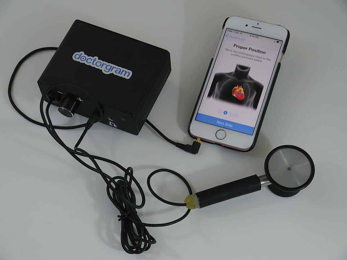
Personalized care: A suite of patented electronic medical attachments enhances a doctor’s “virtual visit”, reducing wait time, eliminating distance barriers and cutting overhead costs. (Courtesy: David Gao)
People are often curious about this approach, and I am sometimes asked how I balance an academic life and an industrial one. In fact, this is quite demanding. I have given up a lot of nights, weekends and holidays, and even so, it would have been extremely difficult to stay motivated without the encouragement and support of close friends, family and my group at UCL. Another common question is “What does your company actually do?” The short answer is that we apply computational chemistry, physics and machine-learning techniques to design and develop new materials for a variety of industrial applications. However, what that statement actually means in practice is not transparent. How does a materials design firm – and a heavily theory-based one at that – fit in to a landscape of chemical, pharmaceutical and electronics companies?
Novel nanoparticles
For Nanolayers, part of the answer lies in the European Union’s Horizon 2020 framework. This framework incorporates a role for companies that are designated as “translators” because they help research groups connect with people in industry who might want to use the group’s software or methods. Our years spent in the theoretical physics community gave us an excellent network of potential university collaborators, while my past life as an industrial materials scientist provided several useful industry connections. Before long, we were invited to join a Horizon 2020 project that aims to replace certain critical, industrially-relevant catalyst materials with novel transition-metal nanoparticles.
Within this project, known as CritCat, our role is to apply machine-learning techniques to results and data collected by our academic partners. We then use our findings to develop catalyst materials that do not incorporate elements such as platinum-group metals, which are of critical importance in Europe due to their cost and scarcity. Our strategy for catalyst design is to figure out what features are relevant in describing these materials and then train neural networks to learn how these features correlate to catalytic activity. This allows us to learn the mechanisms behind what makes a good material, and thus design and control the properties of our materials. We then design new nanoparticles that are subsequently produced by our manufacturing partners and then validated in real-world trials.
As a small-to-medium-sized enterprise (SME) capable of interfacing not only between academia and industry but also between theory and experiment, we hold a unique position within the CritCat project. We have taken a leading role in the dissemination and the exploitation of our technology, and have also leveraged our expertise in computational chemistry and theory techniques to provide additional support services and method development for our theory partners, who are based at Finland’s Aalto and Tampere universities.
Beyond materials science
When I got the opportunity to network with other materials design-focused companies and projects such as NoMAD (novel materials discovery), one of my take away messages was the importance of developing a marketable product along with a diverse skillset. Since Nanolayers’ core values involve performing exploratory research rather than commercializing something that has already been tested, we decided to take on more of a consulting or partner role and looked for an opportunity to apply our expertise and experience in other sectors. Our goal was to use our simulations and machine-learning techniques in an equal partnership with someone capable of producing marketable devices or software.
To this end we recently formed a partnership with two firms (GV Concepts in the US and eQuumSoft in Asia) to develop new technologies for monitoring vital signs and conducting medical pre-screenings remotely. By continuously monitoring patients’ vital signs, clinicians may be able to spot qualitative early-warning signals for a variety of potential illnesses, and intervene if the risk is deemed high enough. The challenge is to do this outside a clinical setting, so that patients – particularly those who are elderly, high-risk or suffering from chronic diseases – can record these vital signs in the comfort of their own homes. This is a complex task, one that involves digital devices, diagnostic tools and complementary vital-signs data-collection software. Our solution will make it possible for patients to monitor their own health in a personalized way using a set of patented diagnostic tools including a digital stethoscope, otoscope, blood-pressure monitor, oximeter, thermometer, ophthalmoscope and camera. These devices are all integrated with a smartphone-based software suite that not only enables patients to connect remotely with healthcare professionals, but also allows doctors to remotely control diagnostic tools during the “virtual visit”.
We use the data collected in this project in a way that is similar to the method we employ for designing novel materials. In this case, we are seeking symptom–disease relationships rather than structure–performance ones, but the strategy of using machine-learning techniques to identify relevant relationships is the same. For example, we use neural networks for image recognition and signal processing to help healthcare professionals interpret the collected data.
As we pick up more projects and partnerships that are structured in a similar way, Nanolayers continues to expand while focusing on the theme of bridging the gap between fundamental scientific knowledge and techniques and industrial applications. In this way, we can enjoy the best of both worlds by exploring new materials and techniques while making sure that the discoveries and advancements we make are applied in a meaningful way. Time spent on improving our own methods and gaining experience is not wasted. After all, one of our most important products will always be the research team itself.
Graphene has many amazing properties, including high strength and stiffness, high conductivity and impermeability to gases, to name but a few. These headline-grabbing properties have generated a considerable amount of hype, with potential new applications announced almost every day. However, as the graphene story has progressed, the task of translating properties measured in the laboratory into commercial applications has proved a greater challenge than many had anticipated. In particular, producing consistent single layers of graphene – the starting point for many potential electronics applications – is a technically difficult task, and doing so on a commercial scale is expensive.
Fortunately, other types of graphene are beginning to prove their worth in other industry sectors. At my firm, Haydale, our focus is on stacks of graphene with 5–100 layers. Materials at the lower end of this range are generally known as few-layered graphene (FLGs), while those at the higher end are termed graphene nanoplatelets (GNPs). When these materials are added to a resin or other thermoplastic material, the resulting mixture can become stronger, and may also become thermally conductive, electrically conductive or both. These enhancements could have applications in many areas, but they appeal particularly to the aerospace industry. Many key aircraft parts are made from carbon fibres bonded together with a thermoset resin. If this resin had better mechanical properties, it might be possible to reduce the number of carbon-fibre layers required – saving weight and thus cost.
Our experiments indicate that substantial improvements are possible: in one recent test, a carbon-fibre composite with FLGs added to the resin showed a 20% improvement in almost all mechanical properties. However, getting there involved much more than simply adding graphene to resin. The key to realizing the well-documented properties of graphene lies in starting with the right material and knowing how to process it for particular applications.
Producing graphene
Graphene can be produced in a number of ways, and individual manufacturers use slightly different processes. One common approach is the “top down” method, where mined organic graphite is exfoliated to produce flakes of fewer layers. Getting down to the desired number of layers may require multiple production stages, since the thickness of most organic materials varies. However, in bulk systems such as the composite inks, pastes and resins we work with, this is not a huge issue.
Alternatively, graphene can be produced layer-by-layer in a “bottom up” method such as chemical vapour deposition using methane gas or another carbon source. This process typically requires operating a reactor at energy-intensive temperatures (900 °C or more), and the reactors must also be cleaned after each batch is produced. Additionally, in many cases the graphene sheets produced by this method are not single layers but FLGs two or three layers thick. Expensive “release tapes” must then be used to peel off individual layers.
Clearly, graphene produced via the top-down method is very different from the bottom-up variety, both in its properties and in its manufacturing cost. However, due to a lack of industry standards, many different carbon nanomaterials can be described as “graphene”. As a result, the prices of similarly labelled products can range from $50 to more than $2000 per kilogram. The temptation is to plump for the cheapest one available, but often this is not the best option. This is because every material produced at the nanoscale is different – in flake size, thickness and, crucially, the types and amounts of chemicals bonded to its surface and ends. These chemical groups are often involved in binding the graphene to other materials, and can thus affect the properties of the mixture. For example, a material with a lot of oxygen groups will act as an insulator, not a conductor. The size and shape of the flakes can also affect thermal conductivity, electrical conductivity and/or mechanical uplift.
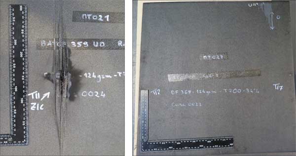
Protective properties The image at left shows the back face of a conventional, unprotected (that is, without copper mesh) composite panel after it was subjected to a severe lightning-strike event. “Punch-through” damage is clearly evident. The image at right shows a similar post-strike image, but in this case the panel had been modified with functionalized nanoparticles, and shows no visible back-face damage. (Courtesy: Haydale Composite Solutions)
In our experience, whatever the desired application, mixing and dispersion know-how is crucial to “functionalizing” graphene (that is, getting other chemical groups to bond with it). Carbon as an additive is inert and does not mix well with other materials, so to get it to disperse in a homogeneous fashion, one needs both a good understanding of functionalization and a detailed knowledge of the particles’ size and shape – which, when the particles are 2–5 µm across, requires special skills and equipment. It is also worth pointing out that adding nanomaterials to other substances does have some potential drawbacks; for example, it could change the viscosity of a resin, which can affect later steps in the production process. Often, there will be a trade-off between the desired performance of the final product and other properties that existed before the nanomaterials were added.
To develop our understanding of these issues, Haydale has conducted an 18-month programme of research in collaboration with Huntsman Advanced Materials using its high-end epoxy resin, Araldite. This work has given us considerable expertise of the mixing and processing techniques required to properly disperse graphene and other nanomaterials into a thermoset or thermoplastic resin. It has also become abundantly clear that adding a second nanomaterial (such as carbon nanotubes or silicon carbide) alongside graphene can have significant effects on performance, over and above the effects of purely adding graphene alone. We believe that this process, which we term “material hybridization”, holds great promise for the future commercialization of composites and, indeed, other materials such as inks.
Taking flight
Since 2014 scientists at Haydale have been using functionalized graphene to improve the performance of carbon-fibre composites in the aerospace industry. This project was based on requirements specified by the Centro Italiano Ricerche Aerospaziali (CIRA), and was managed by an integrated team from CIRA, Haydale and the school of engineering at Cardiff University in the UK, with financial support from the Europe-wide Clean Sky Joint Technology Initiative.
Compared to resins, carbon fibres are immensely stiff and strong, so the structural properties of a component made from a fibre-reinforced composite is dominated by the properties of the fibre, not the resin. Hence, even though adding functionalized graphene to neat resin has been shown to double the resin’s stiffness, one would expect the effect on the macrocomposite to be smaller. Our research investigated the effects of adding both GNPs and carbon nanotubes to resins, and we observed a 13% increase in compression strength and a 50% increase in compression after impact performance. These are both
significant results, since damage resistance and compression properties are of paramount importance in high-performance structures such as composite aircraft wings.
Scientists in Haydale’s composite division (Haydale Composite Solutions) are currently working with industrial partners such as Cobham Technical Services, Airbus and BAE Systems on two research projects that use functionalized nanoparticles to make aircraft components electrically conductive. The first project, Graphene Composites Evaluated in Lightning Strike (GraCELS), is investigating how functionalized nanoparticles affect the conductivity of carbon fibre-reinforced epoxy panels. The GraCELS experiments have shown that adding nanoparticles to the epoxy substantially improved the panels’ electrical conductivity, and greatly enhanced their tolerance of lightning-strike damage. In particular, the modified panels showed no sign of “punch through” damage when subjected to a severe lightning-strike event (see images above).
The second project, known as Graphene-Enhanced Adhesive Technology through Functionalization (GrEAT Fun), is focused on the bonds between carbon-fibre panels in aircraft, rather than the panels themselves. Adhesive bonds made using conventional techniques are generally electrical insulators, which is a problem if we want the structure of the aircraft to conduct electricity. Previous studies have attempted to improve the electrical conductivity of structural adhesive bonds by adding metallic particulates or carbon nanotubes to the bonding material, but these efforts have had limited success in producing bonds that are strong and reliable as well as electrically conductive.
The GrEAT Fun project, in contrast, will use a patented technology for functionalizing GNPs to significantly improve the electrical conductivity of adhesive bonds as well as enhancing the strength of the bonded layer. This functionalized graphene can be incorporated into a thermosetting matrix resin. Inevitably, there will be a trade-off between mechanical and electrical performance and the ease of processing the modified resin; one of the project’s goals is to establish the level of graphene loading that leads to the best overall performance of the adhesive.
Future applications
The aerospace industry is likely to be an early adopter of the adhesives developed during the GrEAT Fun project, but other fields may also benefit. For example, improvements in the electrical conductivity of structural adhesive resin systems could enhance the performance of large off-shore wind turbines, while in the oil and gas industry, conducting resins could make it easier to dissipate static electricity and prevent it from causing damage to pipelines. As for the structural properties of functionalized graphene, there are myriad potential applications, from damage-resistant shower trays to tougher sporting equipment. The transport industry is likely to benefit, too, although here the time frame will be longer due to the regulated nature of the industry. Commercial applications for graphene may have taken longer to emerge than the hype suggested, but these recent developments could finally harness the wonder material’s amazing properties.
An atom interferometer that does not have to be cooled to cryognenic temperatures has been created by physicists in the US. The new device instead employs a cell of warm vapour. The absence of bulky cooling equipment means the device could potentially feature in simple atomic sensors designed for a range of applications – including measuring accelerations with great precision.
Atom interferometers rely on the fact that particles of matter have wave-like properties. Like optical interferometers, they measure the interference fringes produced when the two halves of a split beam are sent along different paths and then recombined. But rather than using components made of matter to split and reflect beams of light, they do the reverse – typically using laser beams to manipulate beams of matter.
Atom interferometers are more sensitive than their optical counterparts because the matter waves they measure travel more slowly than light does. This means that the waves’ phase changes over longer periods of time. This makes them ideal for high-precision measurements, such as looking for variations in the fine structure constant or testing the equivalence principle. They are also used in inertial sensors to make very accurate measurements of position or rotation, for example.
Large and fiddly
So-called light-pulse atom interferometry involves cooling down large collections of atoms to temperatures as low as a few millionths of a degree kelvin. The chilly conditions are needed to reduce the atoms’ range of velocities, so as to increase the signal at the interferometer’s output and keep the atoms closer together to maximize precision. But the lasers and ultrahigh vacuum chambers required to do this are large – the smallest (transportable) systems having a volume of about 1 m3. They are also tricky to operate because they require fine-tuning and must be kept stable.
In the latest work, Grant Biedermann and colleagues at Sandia National Laboratories in New Mexico adopt a different approach involving a vapour of rubidium atoms held at 39 °C inside a 10 cm-long cell. The idea is to reduce the atoms’ velocity spread not by limiting their thermal energy as a whole, but instead by selecting two subsets of atoms with very precise velocities. The researchers did this using two counter-propagating Raman lasers, which first excite the subsets with opposite velocities and then “kick” them along different trajectories to create the interferometer.
Writing in a commentary that accompanies the Sandia group’s paper in Physical Review Letters, Carlos Garrido Alzar of the Paris Observatory in France draws an analogy with optical interferometry. Existing atomic devices, he says, operate like a laser – a coherent source of light – whereas using a warm vapour is like “searching for interferometric effects using the white incoherent light from a common light bulb”.
Flipping spins
To carry out their experiment, the researchers had to overcome a number of technical hurdles. One was how to prepare the atomic states inside their vapour cell. The atoms need to be spin polarized if they are to interfere properly, but their spin can be flipped when they bounce off the cell walls owing to electromagnetic fields created at the surface. To overcome this problem, the researchers covered the walls with a special coating.
Another major challenge was aligning the weak laser beams that were used to detect the interference fringes with the more powerful lasers used to create the interferometer, such that atoms within the two velocity subsets overlapped properly. “Since this really takes place in 3D, angle is critical,” says Biedermann. “So it was a matter of developing optical alignment tricks.”
The scheme’s sensitivity to the phase difference between matter waves travelling along the two arms of the interferometer is limited by the short time it takes thermal atoms to cross the Raman laser beams. With a transit time of just 29 μs, acceleration sensitivity is roughly five orders of magnitude or more below that possible with the best cold-atom interferometers today. However, according to Garrido Alzar, the new scheme does offer “two important advantages” compared with conventional devices. One, he says, is the fact that it can acquire data about 10,000 times more quickly. Another is its ability to measure a broader range of accelerations.
Speedy operation
Mark Kasevich of Stanford University in the US says that the high laser power needed for the interferometer “may be challenging to achieve” in practical devices. But he nevertheless thinks that the scheme’s speedy operation could prove attractive for inertial sensors used to guide cars, for example.
Guglielmo Tino of the University of Florence in Italy also believes that the new research holds promise. “The published results are still very preliminary and the achieved sensitivity is rather low but it will be interesting to see where this method can lead if optimized,” he says. “It might simplify the atomic sensors for several applications.”
There is much more about using atom interferometry to test the equivalence principle in “The descent of mass“.
This week has seen the beginning of Cassini’s Grand Finale. The rather dramatically named final mission for the NASA spacecraft involves 22 dives between Saturn and its surrounding rings. Once complete, Cassini will crash into the planet’s atmosphere in what the scientists hope will be a flurry of data gathering. The spacecraft has already sent back stunning images of storms in Saturn’s atmosphere from its first dive on 26 April. After 20 years since its launch, the mission to Saturn’s system has been a masterclass in space exploration, and NASA highlights the best bits in this theatrical video. The short film, reminiscent of Star Trek, could be considered a bit cheesy, but it’s hard not to form an emotional attachment to NASA’s loyal Cassini as you join in the countdown to its final demise.

 By Matin Durrani