By Tushna Commissariat and Sarah Tesh at LIGO Livingston, Louisiana, US
Being a journalist can be a busy and often stressful job, especially as deadlines loom fast and furious. But one of the best perks of the job is the chance to meet some amazing people and visit some of the best scientific facilities in the world. As most regualr readers of Physics World will know, we – Sarah and Tushna – have been in New Orleans, Lousiana for the APS March Meeting 2017. And it just so happens that about a two-hour drive away from New Orleans lies one half of one of the most advanced experiments in the world – the Laser Interferometer Gravitational-wave Observatory (LIGO) at Livingston.
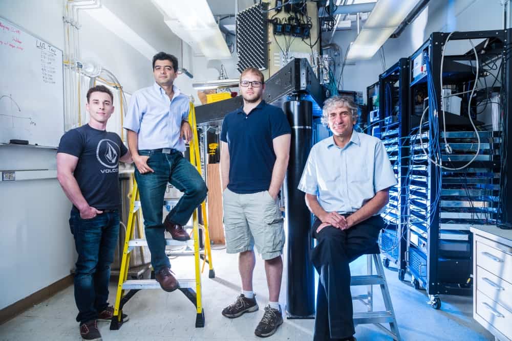
Quantum cohort: John Martinis (right) and some of his team. (Courtesy: Matt Perko)
By Tushna Commissariat in New Orleans, Louisiana, US
“We should have a 20-qubit chip ready very soon… in the next two months most likely,” says Google’s John Martinis to me as we lean against a wall in a relatively quiet corner of the sprawling convention centre in New Orleans. Martinis, a tall man with a mop of silver hair and an Alan Alda-esque manner, is very busy and I’m lucky to have caught him. Earlier that day, he gave one of the APS March Meeting‘s most popular talks on “quantum supremacy: checking a quantum computer with a classical supercomputer”. Martinis, whose team is based at the University of California Santa Barbara, spoke about how they are working towards developing a “scientifically and commercially useful quantum computer” made up of 50 qubits – a 7 by 7 array of superconducting qubits (each of which is coupled to its nearest neighbour) that can be programmed with a one or two-qubit gate – which has an error rate of about 0.1% and can actually do quantum computations.
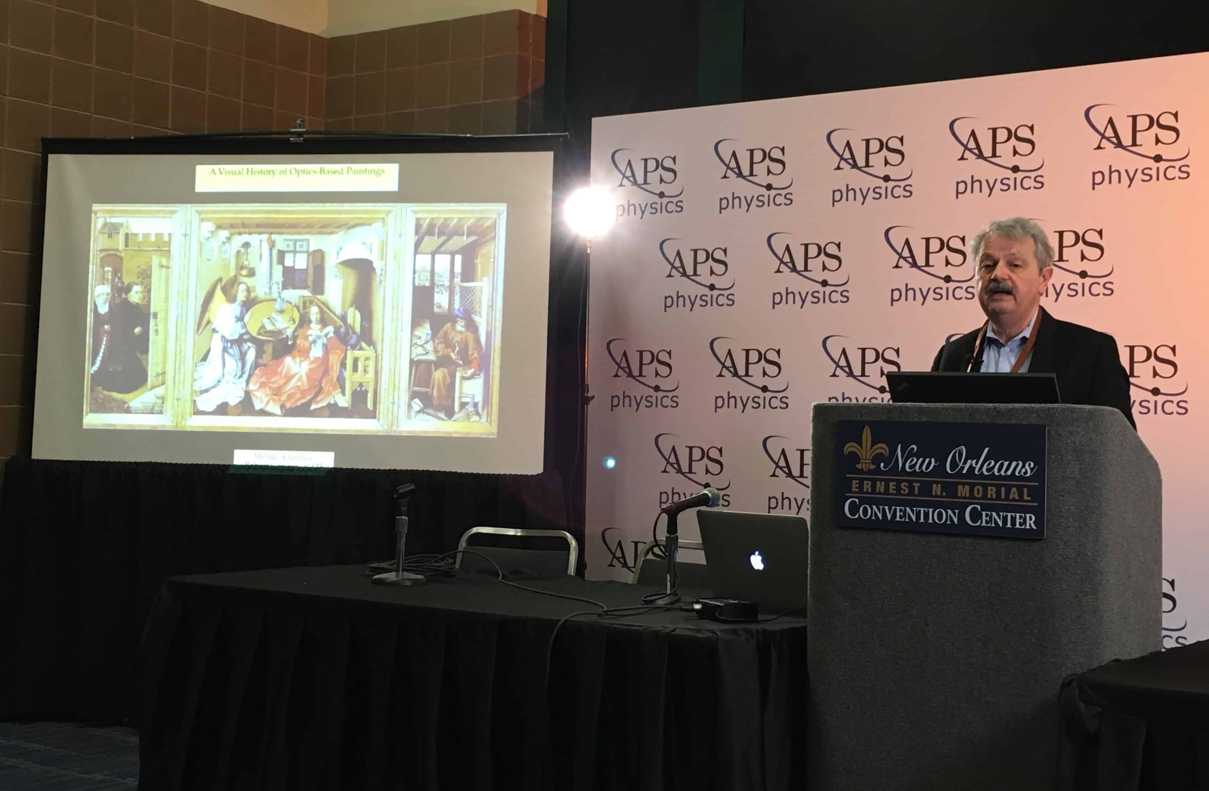
Artists’ secrets: Charles Falco describes how artists used optical lenses. (Courtesy: Tushna Commissariat)
By Sarah Tesh in New Orleans, Louisiana, US
As a physicist who likes to sketch and paint, I love it when art and physics come together. I was therefore excited to see that the APS March Meeting had a variety of talks on the subject. Charles Falco from the University of Arizona in the US told us about his work with the famous artist David Hockney. On a trip to see the 15th century painting The Arnolfini Marriage by Jan van Eyck, Hockney decided that the chandelier was too detailed to have been done freehand. So Falco and Hockney began looking at the intricate parts of paintings by artists through the ages and found that they essentially cheated.
Through focal length and depth-of-field calculations, Falco showed that artists had used optical lenses to project the complicated parts onto the canvas before painting them. They suggest that this has been happening since the 1400s and is a technique used by artists such as Hans Holbein (who painted the iconic portraits of Henry VIII) and Johannes Vermeer (whose work includes Girl with a Pearl Earring). Obviously, they still possessed huge amounts of skill, but it definitely makes me feel a bit better about my own skill level.
Looking ahead: John Ellis on the future of particle physics. (Courtesy: IAI TV)
By Hamish Johnston
In 2012 particle physicists gave themselves a giant pat on the back when the Higgs boson was discovered at the Large Hadron Collider at CERN – nearly 50 years after it was first predicted to exist. But what have particle physicists done since, and what does the future hold for the field? In a video called “After the Higgs boson: what’s next for 21st century physics?” from the Institute of Art and Ideas, the theoretical physicist John Ellis charts the future course of particle physics. Pay attention for a joke about the UK’s foreign secretary Boris Johnson.
I am heading to China tomorrow for a five-day trip in what promises to be a fascinating update on some of the physics that is being carried out in the country.
The purpose of my journey is to gather material for an upcoming special report on China, which will be published later this year.
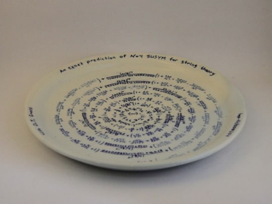
Showcasing science – one of the ceramic items created by Nadav Drukker on show at the new Quantum Ceramics exhibition in London. (Courtesy: Nadav Drukker)
By Matin Durrani
You might not think theoretical physics and pottery have much in common. But they do now, thanks to a new exhibition being staged at the Knight Webb Gallery in Brixton, south-east London, which opens today.
Entitled Quantum Ceramics, the exhibition is the first solo display of ceramic works by theoretical physicist Nadav Drukker. Based at King’s College London, Drukker makes traditional studio pottery as a new way to communicate his scientific research.
Drukker, who is a string theorist, has six different projects – entitled “Circle”, “Cusp”, “Index”, “Polygons”, “Cut” and “Defect” – with each inspired by one of his research papers. His works are all traditional glazed stoneware and porcelain vessels, but decorated with mathematical symbols.
A new way of using self-assembling block copolymers (BCPs) to create patterned nanostructures has been unveiled by researchers in Canada. They found that arrays of BCPs with different lattice spacings can align preferentially to create well-defined moiré superstructures. These superstructures could be used to create optoelectronic devices that self-assemble, allowing device features to be much smaller than are currently possible using conventional fabrication techniques.
BCPs comprise two or more chemically distinct polymer chains connected via covalent bonds. By tuning the molecular weight, chemical composition and the volume fraction of the blocks, researchers can make BCPs that self-assemble into periodic nanopatterns such as arrays of parallel lines and hexagonal dot patterns on a variety of surfaces. Directed self-assembly (DSA) of BCPs by pre-defined templates could lead to patterning capabilities beyond the resolution limits of conventional optical lithography. This could result in components with feature sizes well below 20 nm for use in next-generation optoelectronics devices. Furthermore, the devices could have fewer defects and the process could be less expensive than conventional methods.
New field
DSA is a relatively new field of research and recently a team led by Erik Luber and Jillian Buriak at the University of Alberta and the National Research Council Canada used an array of hexagonal silica dots (prepared via BCP self-assembly) to direct the self-assembly of a second layer of the same BCP. The researchers converted the commensurate, two-layered pattern they produced to a honeycomb pattern of silicon dots that had double the density of the original dots. Now, the team has gone a step further and produced nanoscale structures using the DSA of two incommensurate BCP dot arrays.
“We did this by first depositing the bottom BCP layer as a thin film using a technique called spin coating, followed by solvent annealing to form a highly ordered hexagonal BCP lattice,” explains Luber. “We then converted this BCP lattice to an array of silica dots using reactive ion etching. We repeat this process on top of the same substrate using a different BCP with different lattice spacing. The alignment of the two layers is completely self-directed and is the result of energy minimization between the layers.”
Photonic metasurfaces
The researchers found that the layers align preferentially in a way that produces moiré superstructures – regular patterns created whenever two similar 2D lattices are overlaid – never seen before in DSA. These superstructures contain large, multi-micron-sized grains with preferred majority phases. “Although it is currently unclear what types of applications will make use of these BCP moiré superstructures, one promising application may be photonic metasurfaces with tuneable optical properties,” says Luber.
“We can modify the resultant moiré structure by not only changing the pitch ratio of the two dot lattices but also the dot height and size,” he explains. “We will now be exploring the effect of dot height while keeping all other parameters constant. This study should shed more light on how the moiré patterns form, and help us design these patterns in the future.”
Trump’s 2018 budget proposal concerns US scientists
“The Trump administration’s proposed budget would cripple the science-and-technology enterprise through short-sighted cuts to discovery science programmes and critical mission agencies alike,” says physicist Rush Holt, who is chief executive of the American Association for the Advancement of Science. Holt was responding to US president Donald Trump’s proposed budget for the 2018 financial year, which begins on 1 October. While the document contains only broad details and will probably be modified by Congress, science appears likely to lose out. The Trump administration wants to increase spending on national defence by $54bn to $603bn for the next financial year. This will be paid for by a similar reduction in spending on discretionary items. This includes money for such agencies as the Department of Energy (DOE), the National Science Foundation (NSF), and the National Institutes of Health – all of which are major funders of science. The budget proposal targets DOE programmes apart from maintenance of the national nuclear stockpile for a cut of 17.9% in FY 2018. Funding for the DOE’s Advanced Projects Research Agency-Energy, created by president Obama’s first energy secretary, Steven Chu, is eliminated. The National Institutes of Health, traditionally supported on a bipartisan basis in Congress, would suffer a loss of almost $6bn – about 20%. And the NSF’s funding seems likely to fall by $7bn. NASA, by contrast, stands to lose less than 1% of its funding. But the administration wants the agency to shift its focus more towards “deep-space exploration rather than Earth-centric research”. Supporters of the Environmental Protection Agency (EPA) and environmental research have voiced particular concern because the agency stands to lose 31.5% of its funding. Research at the National Oceanic and Atmospheric Administration (NOAA) also seems set to fall. Its research division stands to lose $126m, representing 26% of its budget.
Strain helps locate quantum dots
A new way of locating tiny quantum dots in a material has been developed by Julien Claudon, Maxime Richard, Jean-Philippe Poizat and colleagues at the University of Grenoble Alpes in France. The technique involves using a piezoelectric transducer to excite resonant vibrational modes of a wire-like antenna structure made of the semiconductor gallium arsenide. Embedded within the antenna is a layer in which the quantum dots – tiny pieces of indium arsenide measuring just 10 nm across – are located in random positions. When illuminated with a laser, the quantum dots emit fluorescent light, the colour of which is dependent upon the mechanical strain on the quantum dot. When the material is set vibrating, the colour of the fluorescent changes with time and also according to the positions of the individual quantum dots. By analysing this information, the team was able to determine the positions of individual quantum dots to a precision of 1 nm. The method could be useful in creating devices in which quantum dots self-assemble in random positions. It could also locate nitrogen vacancies in diamonds and rare-earth ions in crystals. The technique is described in Physical Review Letters.
Estonia to join CERN
Estonia’s minister for entrepreneurship and information technology, Urve Palo. (Courtesy: Albert Truuväärt – Riigikogu Kantselei / Chancellery of the Riigikogu)
Estonia is planning to become a member of the CERN particle-physics lab near Geneva. The Baltic nation has had a co-operation agreement with CERN since 1996, paying around €300,000 to the lab each year. Estonia’s minister for entrepreneurship and information technology, Urve Palo, says that membership would allow Estonian companies to compete with firms from other member states for procurement contracts and that the plan to join CERN will be part of a briefing document introduced into parliament next week. If Estonia became a member, it is expected to pay around €1.4m each year to the lab. Currently, CERN has 22 member states, with Serbia and Cyprus being associate members in the pre-stage to membership.
You can find all our daily Flash Physics posts in the website’s news section, as well as on Twitter and Facebook using #FlashPhysics. Tune in to physicsworld.com later today to read today’s extensive news story on twisted plasmons.
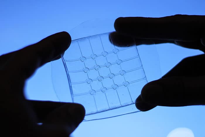
A flexible touch sensor that can distinguish between being touched and being stretched has been developed by researchers in Canada. The devices could be integrated into clothing and could even be used to create “skin” for robots.
Touch sensors are ubiquitous and are used in a range of technologies from smartphone screens to robotic limbs. Researchers are now looking at creating flexible, stretchable sensors that can be used where traditional sensors are not suitable. This raises a challenging problem: if a touch sensor is deformable, how does it know whether it is being touched or stretched? Mirza Saquib Sarwar, John Madden and colleagues at the University of British Columbia (UBC) now think they have an answer, with a sensor with a capacitance that increases when you stretch it and decreases when you touch it.
Delicate touch
Capacitive touch sensors are used on applications like smartphone screens for several reasons. They are very sensitive, requiring a delicate touch rather than a hard press. They can detect multiple fingers touching the screen in different places – essential for many functions of smartphones such as allowing the user to zoom in by moving two fingers apart. The sensors generally comprise a grid of capacitors etched onto glass. Bringing a finger – or a conductive stylus – near one of the capacitors distorts the surrounding electric field, reducing the capacitance.
Stretching out: the new flexible touch sensor is based on a grid of discs and loops. (Courtesy: UBC)
Several groups have produced deformable versions of the capacitive touch sensor. In 2011, for example, researchers at Stanford University in California developed a pressure-sensitive polymer embedded with two networks of carbon nanotubes. Pressing on the device brings the networks closer together, increasing the capacitance. However, stretching the device does the same, so these devices have difficulty distinguishing stretch from touch.
In the new research, the UBC team used two sheets of the dielectric, elastic polymer PDMS embedded with channels of hydrogel parallel to each other but perpendicular to the channels in the other sheet. They made the hydrogel from salt water, allowing it to conduct electricity by the flow of ions. This allows them to create flexible, transparent electrodes in each sheet. Between the two sheets, the researchers embed a third layer of plain PDMS. This electrically isolates the sheets and creates a grid of capacitors where the electrodes cross. Holding the top and bottom layers at different potentials establishes an electric field between them.
Charge develops on your finger because it starts acting as a third electrode
Mirza Saquib Sarwar, UBC
Previous designs for elastic touch sensors have allowed the conductive pathways to pass directly over one another, effectively creating a grid of parallel plate capacitors. However, in the new research, the team intersperses the channels in one sheet with discs and those in the other with loops. Seen from above, the discs sit inside the loops, so the conductive layers are not directly on top of one another. Therefore, instead of passing vertically down through the dielectric layer between the sheets, the electric field spreads much more widely and escapes into the air above the sensor. When a finger approaches, it disturbs the electric field, reducing the capacitance between the plates: “Charge develops on your finger because it starts acting as a third electrode,” explains Sarwar, “So now you have three capacitors – one between the two electrodes and one between each electrode and your finger.”
The researchers demonstrated that the device could still sense touch when being stretched or bent. “When you stretch it, the capacitance goes up,” explains Sarwar, “When you touch one single point, you see the capacitance going down. From that, you can tell that you’ve lightly touched one point while you’re actively stretching it.”
Swiping finger
The sensor could detect multiple fingers simultaneously and track the swiping motion of a finger – potentially allowing smartphone screens and trackpads. The researchers believe the techniques used to make their sensor are amenable to mass production and the materials are cheap and readily available. Sarwar is confident the technology exists to produce pixels with sub-millimetre size, allowing a high-precision sensor. He mentions several possible applications such as wearable technology: “We want to break through the watch idea, so that the whole wrist band can become an interactive surface,” he says. “Also, it could be useful in robotic skin because you’re able to mould it into whatever shape and size you want.”
Danilo De Rossi of the University of Pisa in Italy is impressed, but not stunned, by the research: “It’s nothing particularly new, but the combination of things is certainly worth reading and worthy of attention,” he says.
The most impressive electronics you possess aren’t in your pocket. They’re in your head. Not only does your brain keep you breathing, moving, speaking and thinking enough to read a magazine about physics, but it does it all on the cheap. The brain runs on about 20 watts – less than a light bulb and far less than the megawatts used by supercomputing centres. And yet on this power the brain is able to do things that supercomputers still struggle with, such as advanced pattern recognition.
For decades, scientists have tried to develop “brain-like” code for conventional computers, aiming to emulate the unique talents of the brain. (Imagine what could be achieved by combining the computational power of supercomputers with our own cognitive abilities.) Researchers have, however, found this a very challenging quest, since the architecture of conventional computing hardware is so different from that of the brain. Instead, a community of scientists and engineers is now developing a new kind of computing hardware architecture that is physically, and functionally, more analogous to the computers inside our heads.
Our brain has a plethora of electrically active cells, called neurons, each of which has a profusion of connections, called synapses, to other neurons. With time and experience, the synapses in the brain strengthen and weaken to allow the flow of more or fewer current pulses, which changes the strength, or “synaptic weight”, of connections. Additionally, neurons can be discarded or grown anew, and these structural changes lead to learning and memory. This ability of the brain to adapt and rewire itself, known as its “plasticity”, is why it can learn new tasks without needing an external programmer. Sensibly, the brain has evolved computational strengths that are adapted not so much to abstract computation, but to real-world problems, like not getting eaten by a tiger.
Supercomputers, in contrast, run on switches and logic gates, and can far outperform the brain on computational power alone. This powerful mathematical approach is implemented using semiconductors, which have not only enabled huge advances in computing, but also made it widely affordable. While the brain can rewire its own hardware, this feature is neither replicated nor missed in the main silicon computer-chip industry. The 1980s did see the invention of a hardware component that could be reprogrammed “in the field”, but the “field-programmable gate array” did not prove popular except in niche applications and lacked the full flexibility of neurons and synapses.
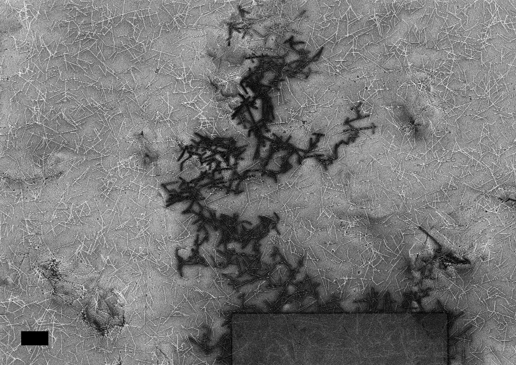
Nanowire networks Films of nanomaterials can be used to create adaptable electronics that mimic the brain, and the connectivity paths through these materials can be imaged using scanning electron microscopy. When the metal electrode (bottom) is connected to electrical ground, nanowires with a conducting path to the electrode and the electrode itself appear dark due to electrons flowing out. In contrast, nanowires isolated from the electrode experience a build-up of electrons, causing them to appear light as more electrons are reflected into the detector. The scale bar represents 10 µm. (Courtesy: CRANN Institute/Jessamyn Fairfield)
Although the raw computational power of supercomputers cannot be matched, Moore’s law, in which the number of transistors on a chip doubles every two years, is slowly eroding. We are perhaps close to the end of gains to be eked from traditional silicon architectures, as we approach the limit of heat dissipation in ever more miniaturized circuits. Another restriction of this technology is that the circuits for computation and memory are kept separate, requiring large throughput to move information from computation to memory and back again. This “von Neumann” bottleneck is avoided in the brain because memory is largely stored in the shape of the network, and in the way in which neurons are connected to which others, rather than as a series of bits that have to be shuttled around.
Deep-learning is effectively a software approach incorporating the brain’s patterns of connectivity to tackle applications like computer vision, speech recognition and language processing
Many impressive forays into simulating the human brain have nevertheless managed to do so using conventional computer hardware. “Deep learning”, for example, is effectively a software approach incorporating the brain’s patterns of connectivity to tackle applications like computer vision, speech recognition and language processing. Deep-learning algorithms often comprise multiple layers of artificial neural networks – sets of software nodes each of which feeds into the next – that can either perform “supervised” learning, involving human guidance, or “unsupervised” learning. Such computational approaches are key to the Human Brain Project, a €1bn European Union initiative to simulate the brain. Deep learning seems to be a promising step towards achieving this goal.
However, trying to implement software for neural behaviour onto traditionally structured electronics is like playing a symphony on only timpanis. How much more could we do if we had electronics that mimicked the timbre and shape of the brain?
Neuromorphic engineering
While the quest to understand how we think, and hence how the brain works, is nearly as old as science, only recently have we developed electronics anywhere near capable of reproducing its circuitry. Early computational devices were based on the binary logic of the transistor, first implemented with vacuum tubes and later in silicon, where bits of information can have values of only 1 or 0. Binary logic is based on algebra first proposed by George Boole in the mid-1800s, an English mathematician working in Cork, Ireland. But in the 1960s Lotfi Zadeh at the University of California, Berkeley, proposed an analogue algebraic system, where a range of less crisply defined values are the basis for logic operations. This “fuzzy logic” is much closer to the changeable synaptic weights of the brain.
One of the first pioneers who saw the relevance of fuzzy logic to biological electronic systems was engineer Carver Mead at the California Institute of Technology, US, who in the 1980s coined the word “neuromorphic” to describe electronic devices modelled on human biology. He went on to create computer interfaces for touch, hearing and vision. While Mead and other early researchers in neuromorphic engineering found niche applications for their devices, ultimately they were limited because most widely available electronics were still based on digital logic using silicon, and the primary industrial goal was to make these silicon transistors as small and reliable as possible.
The memristor can be used as an analogue form of computer memory that is much closer to the plasticity of synapses in the brain
Decades later, a breakthrough result enabled a renaissance in neuromorphic engineering. In 2008 neuromorphic engineers learned of a new circuit element for their arsenal, when a team led by Stanley Williams at Hewlett Packard reported the first experimental realization of a memristor (Nature453 80). This device had first been predicted by Leon Chua in 1971 as a theoretical necessity to complete the set of basic circuit elements: resistor, capacitor and inductor. The memristor in its ideal form is a circuit element whose resistance depends on how much current has previously flowed through it, meaning it can be used as an analogue form of computer memory that is much closer to the plasticity of synapses in the brain.
Hewlett Packard’s implementation of the memristor consisted of a nanoscale film of titanium dioxide, containing positively charged oxygen vacancies, sandwiched between two electrodes. When a current is passed through the film, the oxygen vacancies move one way or the other across the film, depending on the sign of the current. This repositioning of the oxygen vacancies changes the resistance across the film, leading to the device memory.
Mimicking the brain IBM TrueNorth computer chips are based on simulated neurons and synapses. (Courtesy: IBM Research)
While the ideal memristor is a passive device, requiring no power to operate, the experimental realizations of memristors have generally involved some sort of energy storage and release. Since this is required in atomic reordering or chemical reactions at the nanoscale, many researchers say that pure and hence passive memristors are only theoretically possible, though they do say that “memristive systems” like the titanium dioxide film can be implemented as useful circuit elements.
As many researchers realized once the first results were announced, memory of past measurements is a common nanoscale feature. What had previously been seen as a flaw in the electronic behaviour of many nanomaterials could now become a strength. Current flow can often cause small changes in materials, by moving atoms or even just by changing the electron distribution in the material between mobile states and trapped states. These changes may not be noticeable in the properties of a bulk material, but when the material is thin or has a small feature size, the changes can affect material properties in a measurable way. This robust memristance in nanomaterials has thus led to many neuromorphic devices based on nanoscale phenomena and interactions.
Materials for brain-like electronics
The development of memristive devices initially continued in the vein of the thin-film-based Hewlett Packard device, but a variety of other designs soon followed. A phenomenon called resistive switching drives one increasingly popular type of memristor, most notably thanks to work led by Rainer Waser at RWTH Aachen University, Germany, and Wei Lu at the University of Michigan, US. In this device, a conductive filament across a non-conducting oxide can be formed and then strengthened or broken by electrical impulses, allowing patterns of conductivity to be defined and used for either memory or computation. It’s challenging to control the exact filament location and structure, as with many processes at the nanoscale, but these resistive switches are self-healing and responsive to electrical stimuli. The filaments themselves parallel synaptic connections between neurons, whose synaptic weight can be tuned by repeated stimuli. And since filamentary conduction has been found in a wide range of metal oxides at the nanoscale, the exact structure of the device can be tuned for the environment and application.
Polymers are both mechanically and electrically closer to the brain, and have more parallel channels for conduction than inorganic electronics
Another approach to memristors is to combine nanomaterials with polymers, either by coating the nanomaterials with a polymer or by mixing the two. As shown by researchers led by Dominique Vuillaume at the University of Lille, France, polymers in conjunction with conducting nanoparticle or nanowire cores can change their resistance, which is a key feature of memristive devices. Some conducting polymers can also be doped and de-doped, enabling them to act as standalone neuromorphic components when submerged in an electrolyte. Such polymer-based memristors are of special interest for brain–computer interfaces because polymers are both mechanically and electrically closer to the brain, and have more parallel channels for conduction than inorganic electronics. Recent research led by George Malliaras at the École des Mines de Saint-Étienne, France, used derivatives of poly(3,4-ethylenedioxythiophene) (PEDOT) in electrolyte-controlled transistors. These devices have shown both plasticity and another feature of synapses called timing dependence, in which the memristive function depends on how closely spaced together in time the electrical pulses arrive.
These building blocks of neurons and synapses, both the polymer and solid-state implementations, can then be combined into networks that exhibit memory, as shown by researchers led by John Boland at Trinity College Dublin, Ireland. These networks can not only reproduce tunable synaptic weights, but they can also show the same timing dependence as actual synapses do. My own published work with both the Boland and Malliaras labs investigated neuromorphic behaviour in individual nanowires, nanowire networks and polymer electronics, showing that brain-like function can be created in a very broad array of materials and device types. Piece by piece, researchers are reproducing the key components of synaptic plasticity in the brain.
Even the US government has taken an interest in neuromorphic computing, funding the SyNAPSE initiative through the US Defense Advanced Research Projects Agency to the tune of more than $100m. IBM and HRL Laboratories in the US have been the main beneficiaries, with their researchers working to make artificial neurons and synapses in silicon that are compatible with industrial fabrication processes. In 2014 IBM released its TrueNorth chip, which simulates a million neurons and 256 million programmable synapses, while consuming only one ten-thousandth of the energy of a comparable traditional microchip. Computationally, the value of memristive networks is already being shown for conventional tasks such as prime factorization, and novel neuromorphic computing paradigms are also emerging.
The path forward
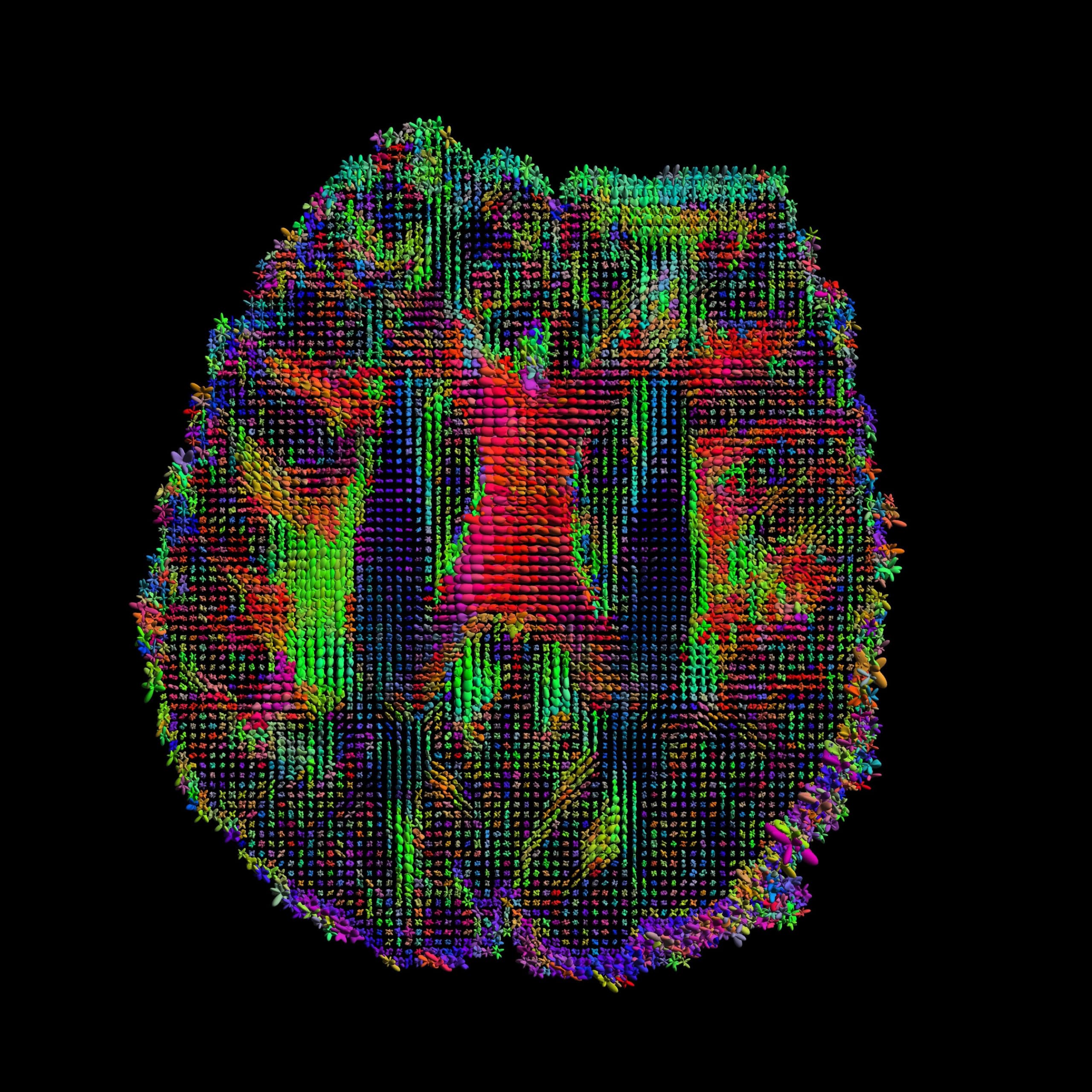
Graphic navigation The Human Connectome Project aims to provide an unparalleled compilation of neural data, such as this high-angular resolution diffusion image of the axial view of a brain. The tensor can be visualized as an ellipsoid in 3D space, showing fluid mappings and brain connectivity. (Courtesy: Laboratory of Neuro Imaging and Martinos Center for Biomedical Imaging, Consortium of the Human Connectome Project – www.humanconnectomeproject.org/David Shattuck and Paul M Thompson)
While this is all exciting research, many important unanswered questions still lie beneath the surface. Which brain features are actually necessary for computing, memory or – dare we ask – consciousness? Which parts of the connectivity of the brain are critical, and which are remnants of our evolution that we no longer need? Does the brain run on electrical pulses merely out of biological necessity, or for computational reasons we have yet to realize and exploit? And even if we can reproduce the behaviour of synaptic spikes in artificial neuromorphic devices, will we gain anything from it without a way to crack the neural code that determines how these spikes are translated into movement, feeling or memory?
To find a path forward, neuromorphic engineers must talk to neuroscientists who have long approached these questions from the other side, examining fully formed and functioning brains and attempting to tease out the principles underneath. Those looking to build a brain from the ground up would be foolish not to seek out this knowledge. The amazing work coming out of the Human Connectome Project in the US, for example, has shed new light on how different regions of the brain are interconnected, light which could illuminate a new path for neuromorphic device connectivity. Only then can the scientific community get closer to the tantalizing dual prizes, of computers that can truly grow and learn, and a better understanding of the computers at work inside our very own heads.