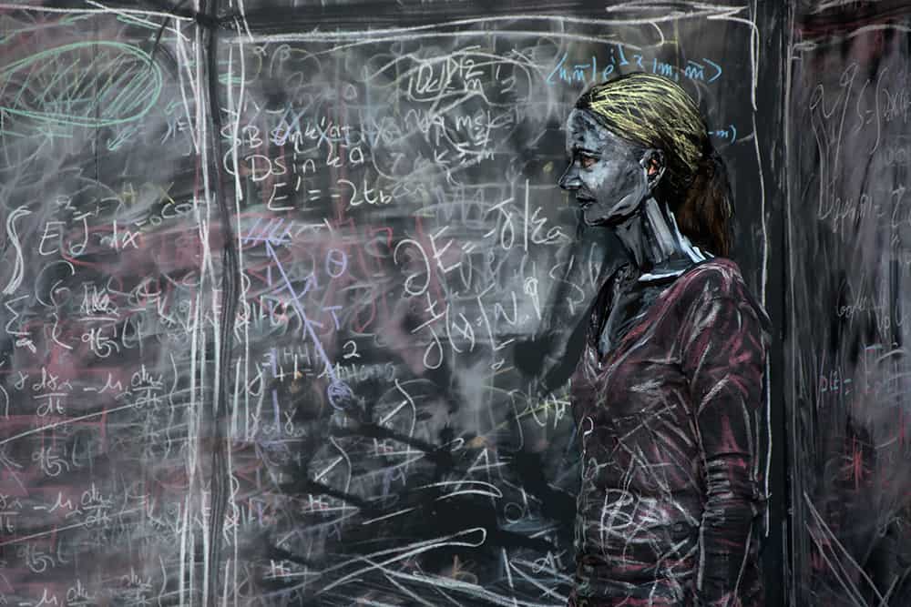
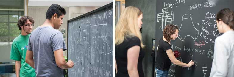
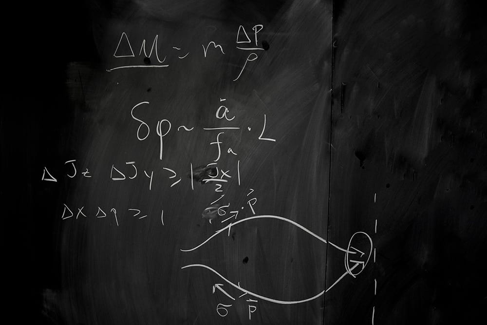
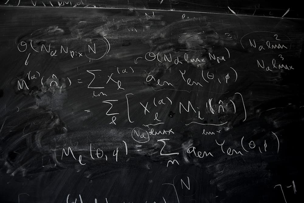
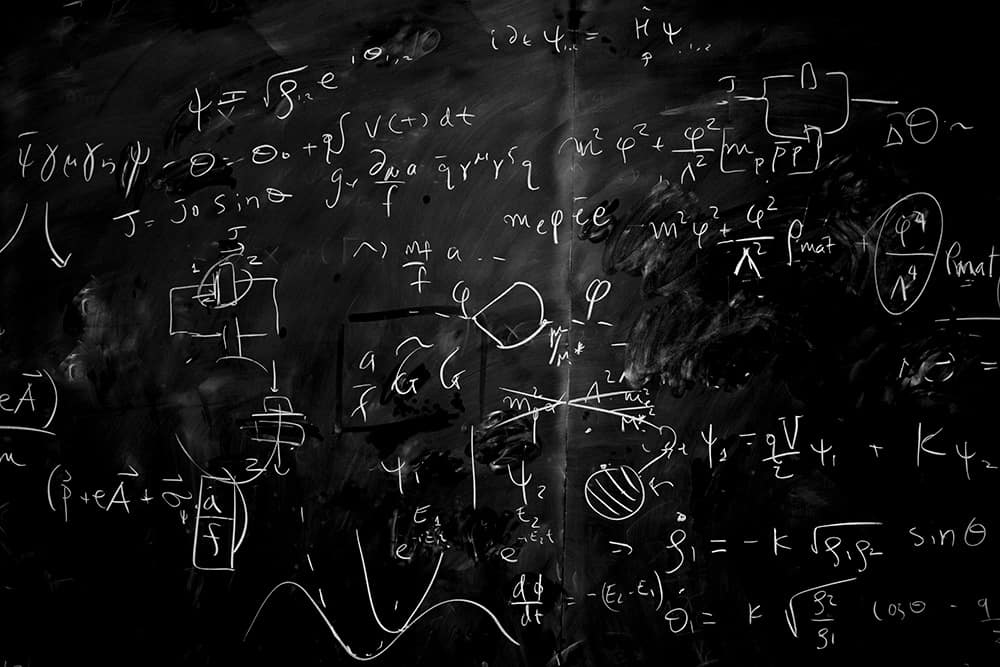
Can you tell what branch of physics is being described on the blackboard above? It’s one of six photographs taken by the communications folks at the Perimeter Institute for Theoretical Physics in Waterloo, Canada, where blackboards are an integral feature of the building’s design, appearing everywhere from the lifts to coffee areas.
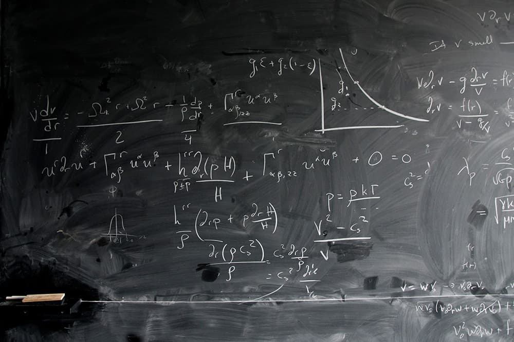
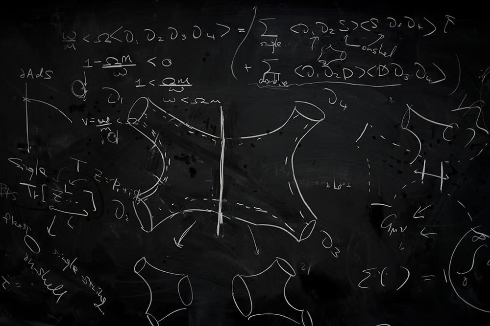
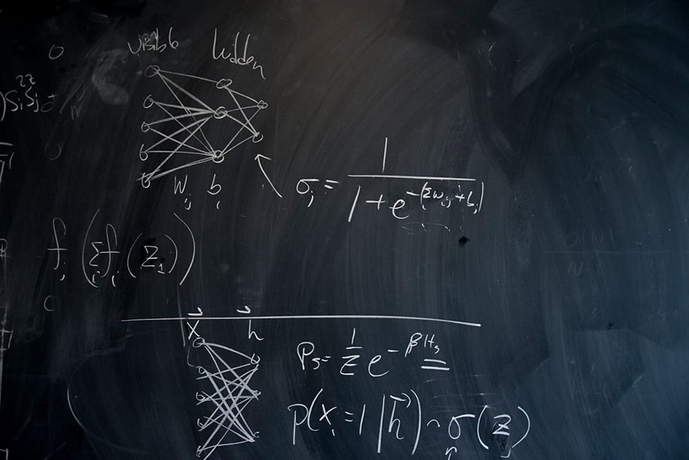
In this quiz, your task is to study six blackboards and match them up with the physics topics they represent. There’s no prize, other than the satisfaction of having at least some inkling of what those clever theorists at the Perimeter are up to.
So here are the six topics:
• Accretion physics and general relativity
• Cosmology
• Neural networks and condensed matter
• Particle physics 1
• Particle physics 2
• Strings
And here are the six blackboards (you can click on each to see it in more detail).
BLACKBOARD 1
BLACKBOARD 2
BLACKBOARD 3
BLACKBOARD 4
BLACKBOARD 5
BLACKBOARD 6
We’ll reveal the answers at the end of the month. In the meantime, please don’t spoil the quiz for others by revealing the answers in the comments.
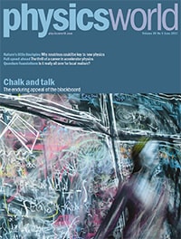
You can find out more about the power of blackboards in a great feature in the June 2017 issue of Physics World by science writer Philip Ball, who reckons that the blackboard still
retains an aura and usefulness for physicists that more advanced technologies can’t match.
Remember that if you are a member of the Institute of Physics, you can read Physics World magazine every month via our digital apps for iOS, Android and Web browsers.
Fermilab mades its name with the Tevatron proton–antiproton collider but neutrinos hold the key to the lab’s future, as Ben Still from Queen Mary University of London makes clear in a feature on the physics of these elusive particles.
You can also enjoy a cracking review of Tommaso Dorigo’s new warts-and-all account of life in the CDF collaboration at Fermilab, while Seyda Ipek from the lab pops up in Philip Ball’s homage to the blackboard – which you can also read on physicsworld.com.
Plus don’t miss this month’s Lateral Thoughts, which reveals how one physicist working in a Scottish call centre ended up chatting to Enrico Fermi’s daughter-in-law about her TV.
Remember that if you’re a member of the Institute of Physics, you can read Physics World magazine every month via our digital apps for iOS, Android and Web browsers.
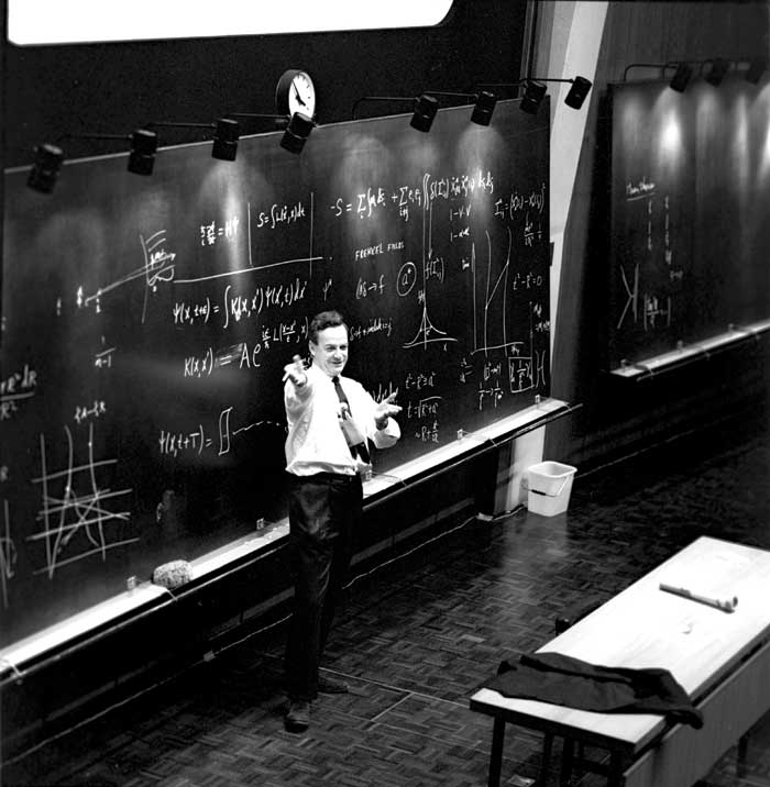
Do an online image search for Richard Feynman. Go on, try it now. What do you notice?
He’s a photogenic sort of guy, of course: that puckish smile, the twinkling eyes, the exuberant mane of hair. But what is most noticeable is that Feynman is often standing in front of a blackboard – usually adorned with squiggles that most physicists will identify as the notation of quantum mechanics.
While looking through images of famous physicists for a forthcoming book on quantum theory, I was struck by how often the blackboard is their backdrop. From Albert Einstein and Niels Bohr to Werner Heisenberg and Paul Dirac, all have their “blackboard portrait”. Sure, experimentalists are usually depicted surrounded by lab equipment, but it seems we have decided nothing announces “theoretical physicist” as clearly as the blackboard. What’s going on?
When thoughts become real: physicist Lauren Hayward Sierens captured as a real person in The Living Chalkboard artwork at the Perimeter Institute for Theoretical Physics in Waterloo, Canada. (Courtesy: Alexa Meade/Perimeter Institute)
Teaching tool
The profession-defining pose is an old idea. Back in the 19th and early 20th centuries, chemists – from Louis Pasteur to Marie Curie – were commonly photographed or painted holding aloft a flask and gazing nobly at its contents. It was a gesture that actually derives from a rather unheroic tradition: physicians in the late Middle Ages and the Renaissance would typically be depicted diagnosing their patients by a visual inspection of their urine.
Physics is a younger discipline, barely recognized in today’s sense until the 19th century. And theoretical physics is more recent still – Einstein’s generation was the first to make it a distinct endeavour. But by choosing the blackboard pose as the archetypal image of the physicist, we seem to be saying that physics is inherently cerebral, defined by abstract mathematical ideas inscribed in chalk.
That conception probably owes a great deal to Einstein himself. As the French literary theorist Roland Barthes explained in 1957: “The historic equation E = mc2, by its unexpected simplicity, almost embodies the pure idea of the key…opening with a wholly magical ease a door which had resisted the desperate efforts of centuries.” And popular imagery, Barthes continued, faithfully expressed that idea. “Photographs of Einstein,” he wrote, “show him standing next to a blackboard covered with mathematical signs of obvious complexity; but cartoons of Einstein…show him chalk still in hand, and having just written on an empty blackboard, as if without preparation, the magic formula of the world.”
The evocative power of the equation as a “magic formula”, as if it is some gnostic incantation to unlock the secrets of the universe, is an image with roots in the Renaissance tradition of natural magic. But why should writing it on a blackboard make it so potent?
Black to basics
The invention of the blackboard is popularly attributed to a Scottish schoolteacher named James Pillans, who early in the 19th century placed many slate tablets side by side so that the old practice of writing on them with chalk could convey more complex information and illustration. But these writing devices might be much older. “I have heard that blackboards originated in India”, says theoretical physicist Harsh Mathur of Case Western Reserve University in Cleveland, Ohio, who adds that the famous Persian traveller Al-Biruni wrote about their use in the 11th century.
Whatever their origin, by the mid-1800s these boards were made instead from wood coated with a thick black paint, which could be wiped clean with dry rags or felt erasers. And while the appeal of a cheap, erasable surface for displaying large words and diagrams in high-contrast markings might not seem particularly mysterious, anyone who has ever used a blackboard and chalk knows there is more to it than that.
A place to collaborate: the Perimeter Institute for Theoretical Physics was designed with blackboards everywhere, even in the lifts. (Courtesy: Gabriela Secara)
Make an error in your spelling or calculation and – swish! – it’s gone, as if you’d never made the slip at all. There are no electronics to malfunction or bulbs to burn out, as was often the case with the overhead projectors that once sought to usurp the blackboard’s role. It’s easy to edit the surface, leaving parts of what you’ve written while erasing others. And there’s no more satisfying way of starting afresh on a problem than wiping your earlier thoughts with a damp cloth to return to that light-absorbing void.
Sure, whiteboards don’t cloud you in dust, but nor do they capture the same aesthetic. Perhaps, given the white or pale walls of most academic environments, whiteboards don’t sufficiently demarcate a space for thinking from the distractions of the surroundings. Besides, the pens smell and dry up, they slip and slide on the shiny surface, and they’re easily smudged. Worse, you can never quite get the damned boards clean: there’s always a faint residue, the distracting whisper of someone else’s ideas.
Blackboard and chalk – like paper and ink – are a combination that modern technologies can’t improve or displace. You still see blackboards (and plenty of whiteboards too, it’s true) in physics research centres across the world. At the Perimeter Institute for Theoretical Physics in Waterloo, Canada, they’re an essential element of the design, being installed in the lifts and coffee areas of the original building. The Isaac Newton Institute for Mathematical Sciences in Cambridge, UK, even has blackboards in the toilets; you never know when insight might strike.
This ubiquity can create a sense of community and shared endeavour, as if the creative thoughts of one’s peers seep into the very walls. “The evidence of past conversations can be inspiring”, says Lauren Hayward Sierens, a condensed-matter physicist at the Perimeter Institute. “Often what you’ll see on a given blackboard at the Perimeter is a combination of many different conversations. I can rarely understand these past conversations if I wasn’t a part of them, but it’s inspiring nonetheless to be surrounded by so many ideas.”
Chalk and talk
For Seyda Ipek, a particle physicist at Fermilab, blackboards are such a part of her everyday life that talking about them is like discussing how one drinks water. “You don’t think about it until it is pointed out,” she says. “At Fermilab both offices and common areas are filled with blackboards and whiteboards. My previous institution, the University of Washington, also had blackboards everywhere, including hallways.”
Ipek says that these surfaces promote informal, impromptu communication and discussion. “We have a whiteboard in our coffee lounge. While we have our after-lunch coffee, we often use it. Someone asks ‘What’s new?’ and then someone else goes up to the board and says ‘I’ve been thinking about this lately. Let me show you.’”
Quite simply, the blackboard is a democratic space, where ideas can be easily shared. “Two people can’t bend over a notebook to discuss,” Ipek points out. “The board gives ample space and it is generally understood that anyone can go up to the board. Sometimes people do that to clarify their misunderstandings, or to challenge each other. Duelling with ideas at the blackboard is not uncommon.”
That kind of intellectual sparring might be hugely facilitated by this shared canvas for thinking on. If someone claims your idea is wrong, you might feel attacked and respond defensively. But if your ideas are chalked on a board, you and your colleagues can scrutinize them almost as an impersonal object of study. Over at Case Western, Mathur believes that the ease of erasure makes students less hesitant to put down answers on the board. “Perhaps it’s the impermanence of writing on a board that makes them feel less concerned about being judged negatively,” he says.
Using a blackboard also moderates the pace of a discussion or explanation. Blackboards help in teaching by slowing down the lecture and allowing the students to absorb information and knowledge at a more human rate. Students in Mathur’s first-year introductory physics class overwhelmingly favour the blackboard over PowerPoint as the primary means of communication.
The time and effort involved in using a blackboard can be good discipline for communication too. PowerPoint speakers who flash up slide after equation-packed slide would have to speak more slowly and think twice about what to include if forced to write everything out by hand. Blackboards, Ipek notes, regulate one’s talking speed and give the audience time to absorb the ideas and ask questions. “At Fermilab we have a journal club where each week one person gives a blackboard summary of an interesting paper. One week we had a talk with slides, and everyone complained.”
There’s also something about a blackboard that seems to fit with the way the mind works: sketching, erasing, supporting a free flow of ideas. “Many physicists like to do a back-of-the-envelope calculation before delving deeper into a computation, and blackboards are a great tool for that”, says Tibra Ali, another theorist at the Perimeter Institute. Indeed, there’s a trophy-like quality to a clever piece of work prominently displayed on a blackboard. Some physicists like transcribing a hard-won solution onto a blackboard to understand the full ramifications – and perhaps just to gloat.
The physics pose: Richard Feynman is just one of countless theorists caught on camera in front of a blackboard. (Courtesy: CERN)
If it ain’t broke…
Despite their low-tech nature, blackboards seem to be working together with new technologies. Ali, for example, says that he and his collaborator often do computations on a blackboard and take an image of them with their mobile phones before erasing the writing and moving on to the next step. “Many a time,” Ali says, “the main idea or the main computation for a project that becomes a paper happens while we are doing these intense computations on a blackboard.”
Given that the blackboard appears to be an optimized technology, tampering with it might seem to be a bad idea. Designers of the new Stephen Hawking wing of the Perimeter Institute thought they knew better, installing a special glass in the discussion areas when it opened in 2011. Opaque but bright when viewed from the front, the glass becomes transparent from the side. “The idea was to have an open bright space with natural light but at the same time have the glass serve as whiteboards on which physicists can write with markers,” recalls Ali.
But the physicists didn’t bite – and eventually old-fashioned blackboards were placed in those discussion areas instead. Likewise, when shiny PVC blackboards, requiring special pens, were installed at the National Graphene Institute at the University of Manchester, UK, to eliminate “dangerous” chalk dust, they were barely used. Squiggles written on a visit by then British chancellor George Osborne were later accidentally wiped by an over-eager cleaner.
There are, then, plenty of practical reasons why blackboards are great tools for thinking, collaborating and communicating. But as Barthes hinted, their significance for physics goes beyond the pragmatic. Displayed at epic scale on walls, blackboards can’t help but exude power, authority and even artistry. With their imperfectly erased ghosts of equations past, they remind us of medieval palimpsests: documents on vellum that, too expensive to discard, were scraped almost clean for reuse while still carrying the tantalizing traces of other thoughts in other minds.
Like historical relics and works of art, blackboards may themselves become venerated objects, imbued with almost mystical significance. The blackboard used by Einstein when he gave three lectures on general relativity at the University of Oxford in 1931 has been preserved as a historical artefact at the Museum of the History of Science in Oxford. (There used to be two blackboards, but one disappeared “in mysterious circumstances”, according to former museum director Jim Bennett.) The board shows Einstein’s calculations of the age, size and density of the universe, and it has become the most famous object in the collection. “People come to the door of the museum and say ‘Where is Einstein’s blackboard?’,” says Bennett. “It’s become a sort of icon. People come and look at it as if is was almost a sort of quasi-religious object.”
We do that to other historical artefacts of science too, of course – Michael Faraday’s induction coils, Galileo’s wooden ramps, a first edition of Isaac Newton’s Principia. But a blackboard used by a legendary scientist has a unique aura, not just because the equations and diagrams were traced in perilously fragile chalk dust by their own hand but also because these markings seem like a trace of thought itself. Like thoughts, they can be fleeting, they can vanish at the stroke of a hand. Yet here they remain: the magic formulae of the world.
Feynman’s blackboard at the California Institute of Technology was photographed at the time of his death in 1988, and seems almost tailored to serve as an epitaph for the great scientist. “What I cannot create I do not understand,” he had written – followed by what might be seen as a corollary: “Know how to solve every problem that has been solved.” Feynman might just as well have written these thoughts in his notebook. But how much more mystique and pathos they acquire on a blackboard.
The art of the blackboard
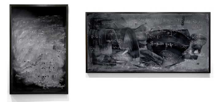
Physics in action: blackboards photographed by Spanish artist Alejandro Guijarro at Stanford University (left) and the University of California, Berkeley (right). (Courtesy: Alejandro Guijarro)
It was the allusive quality of semi-erased blackboards that appealed to Alejandro Guijarro, a Spanish artist who has taken a series of photographs of physics blackboards that he found in lecture halls and researchers’ offices at CERN, and university institutes in Oxford, Cambridge (UK), Stanford and Berkeley. These images, Guijarro has explained, “are fragmented pieces of ideas, thoughts or explanations from which arises a level of randomness”. He admits that he didn’t understand any of the physics but selected the blackboards purely on aesthetic grounds. “I was interested in the action, the gestures and the marks on the surface” – which he looked at as one might the brushstrokes in an abstract painting.
Given their size and their public nature, blackboards can become almost a “performance space” for the physicist. The performative human traces left in blackboard inscriptions were the subject of an art installation commissioned by Canada’s Perimeter Institute for Theoretical Physics in 2015. Artist-in-residence Alexa Meade created a “room” that was one gigantic blackboard, in which not only its walls and armchairs but also two live researchers became the dark surfaces covered with inscribed lines and symbols and the expressionist smears of erased chalk. Meade made her blackboard “universe” after first immersing herself in the culture of the institute, attending lectures and talking to the scientists.
“I think Alexa’s work captured the fundamental connection between the blackboard and the theoretical physicist, illustrating how the blackboard allows a physicist to put his or her thoughts and ideas into a new form,” says Lauren Hayward Sierens, who was one of two Perimeter scientists enlisted by Meade as a human blackboard. It’s hard to imagine whiteboards having quite the same visual appeal for artists.
Watch artist Alexa Meade create The Living Chalkboard with Perimeter Institute physicists. For more about this project, see the Perimeter Institute website. (Video courtesy: Alexa Meade/Perimeter Institute)
A camera made by combining graphene with industrial semiconductor processing has been unveiled by researchers in Spain. Their device is sensitive to a wider spectrum of light than any commercial camera and the team says that the new process could also be used to create high-speed optical interconnects for communications networks.
Graphene is a sheet of carbon just one atom thick and this “wonder material” has a number of very useful electronic properties, such as an extraordinarily high electron mobility. As a result it has been used to create displays, loudspeakers, touchscreens and other electronic devices. However, most of these applications are in the early stages of development and researchers and companies are still working on how to integrate graphene into industrial-scale manufacturing processes.
Today’s electronics industry is dominated by the complementary metal-oxide semiconductor (CMOS) process, which combines silicon with metals and insulators on single wafers that can contain billions of transistors. Integration of other semiconductors such as graphene into CMOS, however, poses a problem because the lattice mismatch between different materials usually makes it impossible to grow high-quality layers of other semiconductors on silicon. Indeed, when graphene electronic devices have been created, they have not been integrated into CMOS circuits.
Limited range
The inability to integrate other semiconductors puts restrictions on the performance of CMOS-based cameras. “The camera in your smartphone can only see visible light as silicon only absorbs visible light,” explains Frank Koppens of the Institute of Photonic Sciences in Barcelona. “If you want to detect infrared light you have to buy an indium gallium arsenide camera, for example. That will cost you around $40,000 or $50,000 because indium gallium arsenide is not monolithically integrated with CMOS, so they have a very complicated process to integrate the readout circuit with the photodetectors.”
In 2011, Koppens and colleagues produced a high-sensitivity photodetector for both infrared and visible wavelengths by attaching two electrodes to a sheet of graphene covered with lead sulphide quantum dots. Photons absorbed in the quantum dots create electron-hole pairs. The electrons were retained in the quantum dots, while the holes moved down into the graphene, dramatically increasing its electrical conductivity and producing a large increase in current. However, the researchers could not then go on to produce a camera. “A photodetector you can just wire up to an electronic board,” explains Koppens. “A camera needs to read out one million photodetectors at the same time, so you need a micro-electronic circuit.”
In the new work, Koppens’ team transferred graphene epitaxially grown on copper foil onto the surface of a silicon CMOS chip. The chip was embedded with the circuitry to read out each camera pixel individually. They then patterned the graphene to define each pixel and deposited a layer of quantum dots on top. The resulting camera can detect wavelengths from 300 nm (near-ultraviolet) to 2000 nm (short-wave infrared). Even though the graphene is not used to absorb the light, its extraordinarily high electronic mobility produces a stronger signal, which allows it to detect infrared light above noise where other devices cannot. The researchers believe the device could find use in cameras for smartphones, security systems, vehicles, and food and pharmaceutical inspection systems. Crucially, its integrated CMOS production could make it no more expensive than current smartphone cameras.
Unprecedented speeds
The researchers are also working to produce graphene-based optical interconnects, which could boost the capacity of optical communications networks and even lead to optical computers. Although, in the current design, the quantum dots limit the speed of the camera, graphene itself can absorb light – albeit much less effectively – at unprecedented speeds: “For data communications you need to integrate graphene with silicon photonics,” says Koppens. “That’s also a silicon CMOS-based technology.”
Andrea Ferrari of the University of Cambridge in the UK told Physics World, “The most important result [of the research] without any doubt is the first bona fide, large area graphene-CMOS integrated device”. Ferrari, who was not involved in the research, adds: “This is the last challenge when it comes to graphene optoelectronics.” He says one of the next big hurdles will be to develop a production process suitable for “fabs” – the billion-dollar production facilities that produce commercial CMOS chips. “If graphene-CMOS integration actually works properly in the fab, then we are done: we are looking at a major revolution, with optoelectronic devices in your phone, in data transmitter units for the internet of things – all based on graphene,” he says. “This is a major result”
Photons in relatively weak beams of light could be made to interact with each other by shining them through a piece of silicon with a specific set of voids cut through it. That is the conclusion of Hyongrak Choi, Mikkel Heuck, and Dirk Englund of the Massachusetts Institute of Technology in the US. They have done calculations that suggest a weak beam of light can create strong electric fields within a piece of silicon that contains a precise arrangement of nanometre-sized voids. The field can be as much as 10,000 times the strength of the electric field normally associated with such light. The presence of such a field would allow a photon to modify the index of refraction in the region that surrounds it. A second photon travelling through this region would be affected by this change – the result being an interaction between the photons. Normally, extremely intense laser light is required to create this effect. The ability to interact photons within much weaker light beams could lead to the development of new types of switches and other devices to create fast and energy-efficient optical communications networks that do not require electrical components. The effect is described in Physical Review Letters and could even be used to create devices for quantum computers in which information is encoded into photons.
Plasma drives high-gain laser amplifier
Vulcan laser target area at the Central Laser Facility showing the set-up for the plasma laser amplifier. (Courtesy: University of Strathclyde)
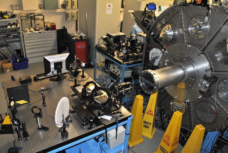
A plasma-based amplifier of laser light is described by its creators as having the highest ever gain. Built by an international team led by Dino Jaroszynski at the University of Strathclyde, the system takes picosecond-duration laser pulses carrying just a few picojoules of energy and boosts them up to about 100 mJ – which is a gain of about 100 million. The amplifier uses high-energy 100 J laser pulses at the Vulcan laser at the UK’s Central Laser Facility in Oxfordshire to create a plasma by firing the laser at a jet of hydrogen gas. The picojoule laser pulse to be amplified is fired at the plasma, where it collides with a high-energy laser pulse. The collision produces a beat wave of light that drives plasma electrons into a regular pattern that mimics the beat wave. This wave sweeps up the energy of the high-energy pulse and outputs it into the low energy pulse, resulting in a huge amplification of the low-energy pulse. An important feature of the amplification process is that the duration of the low-energy laser pulse is not increased significantly during the amplification process. “Our results are very significant in that they demonstrate the flexibility of the plasma medium as a very high gain amplifier medium,” says Jaroszynski. “We also show that the efficiency of the amplifier can be quite large, at least 10%, which is unprecedented and can be increased further.” However, he points out that random fluctuations in the plasma are also amplified, which contributes to noise in the amplified pulse. The team believes that plasma-based amplifiers could play important roles in the development of the next generation of high-power lasers. The research is described in Scientific Reports.
Astronomers have discovered galaxies in the early universe that are creating stars more than a hundred times faster than the Milky Way. These rapidly growing galaxies formed less than a billion years after the Big Bang but are so distant that their light is only just reaching Earth, where it has been observed by researchers using the Atacama Large Millimeter/submillimeter Array (ALMA) in Chile. Roberto Decarli of the Max Planck Institute for Astronomy in Germany and colleagues were originally investigating star formation in very distant galaxies with quasars – the supermassive black holes at the centre of massive galaxies. “But what we found, in four separate cases, were neighbouring galaxies that were forming stars at a furious pace, producing a hundred solar masses’ worth of new stars per year,” Decarli explains. The Milky Way only forms one solar mass per year and other early universe galaxies had star formation rates between one and 10 solar masses per year. “Very likely it is not a coincidence to find these productive galaxies close to bright quasars,” says team member Fabian Walter. “Quasars are thought to form in regions of the universe where the large-scale density of matter is much higher than average. Those same conditions should also be conducive to galaxies forming new stars at a greatly increased rate.” The team suggests this chance discovery may explain a cosmic mystery – a population of massive elliptical galaxies from when the universe was 1.5 billion years old. Astronomers had been puzzled about how these had formed so many stars so quickly, but the newly found hyper-productive galaxies may be the answer. To determine if this is the case, follow-up observations will investigate how common this new type of old galaxy is. Also presented in the Nature paper, the ALMA observations showed the earliest known example of two merging galaxies.
Xmon quantum processor solves linear equations
X factor: the processor comprises four xmons, which appear in orange, blue, green and red in this composite image. (Courtesy: Y Zheng et al./Phys. Rev. Lett.)
Physicists in China are the first to use a superconductor-based quantum processor to implement a quantum algorithm for solving linear systems of equations. Yarui Zheng, Chao Song and Chao-Yang Lu of the Chinese Academy of Sciences and colleagues ran the HHL algorithm on a processor they built. It comprises four superconducting “xmon” qubits – which store quantum information in terms of the number of superconducting Cooper pairs held within each qubit. The HHL algorithm was devised in 2009 by Avram Harrow, Avinatan Hassidim and Seth Lloyd, and is able to solve a system of linear equations with N variables in a running time that scales with the logarithm of N. This is much faster than the best classical algorithm, which has a running time that scales with N. Solving large-scale systems of linear equations is crucial in many fields of science and engineering, and therefore there is great interest in developing a practical quantum computer that could perform this task. The HHL algorithm has already been demonstrated in quantum processors based on photons and nuclear magnetic resonance. However unlike xmon-based systems, both these technologies are not easily scaled-up for solving practical problems. While the team’s four-qubit system offers no advantage over a classical computer, they write in Physical Review Letters that “the superconducting quantum circuits could be used to implement more intricate quantum algorithms on a larger scale and ultimately reach quantum-computational speed-up”.
Construction begins on European super telescope
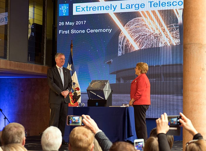
First stone: Chile’s president, Michelle Bachelet (right), and Tim de Zeeuw, director general of the European Southern Observatory, mark the start of construction for the $1.5bn European Extremely Large Telescope. (Courtesy: ESO / Juan Pablo Astorga)
Work has begun on a huge telescope that will capture 15 times more light than any other optical telescope currently in existence. The $1.5bn European Extremely Large Telescope (E-ELT) is being built by the European Southern Observatory (ESO) on top of a 3 km-high mountain at Cerro Armazones in the northern Chilean Andes. The E-ELT will feature a 39 m primary mirror while the telescope’s secondary mirror will be up to 4 m in diameter. When complete in 2024, the E-ELT’s seven science instruments will study galaxy and planet formation as well as planets orbiting other stars, including probing their atmospheres using spectroscopic measurements. The “First Stone” ceremony to mark the start of construction was attended by Chile’s president, Michelle Bachelet, who noted that the E-ELT is “more than a telescope”. “It marks one of the greatest expressions of scientific and technological capabilities and of the extraordinary potential of international co-operation,” she adds.
The atomic structure of an irradiated material is closer to a liquid than a glass, according to a team of researchers in the US. Glasses have been used by researchers to study and predict possible effects of radiation damage, but the engineers behind the new research say that studying liquid states may be more appropriate. They add that the findings from their molecular-dynamic stimulations could help to identify novel radiation-resistant materials.
Exposure to neutron radiation can cause significant structural damage to materials. Understanding the effects of this damage is important for applications such as the construction of nuclear facilities, and the storage of nuclear waste.
“When exposed to radiation, materials undergo some disordering of their atomic structure,” explains Mathieu Bauchy, a civil engineer at the University of California, Los Angeles (UCLA). “In turn, this disordering can affect properties such as density, stiffness, strength and toughness. Therefore, it is essential to understand the effect of irradiation on the atomic structure of materials in order to ensure their integrity.”
The disordered atomic network resulting from irradiation resembles the disordered non-crystalline state of glassy materials. Glasses are formed when a liquid material is rapidly cooled, or quenched, through a process known as vitrification. Instead of forming an ordered crystalline solid, the rapid cooling causes the atoms to become stuck in a non-crystalline state.
Irradiation versus vitrification
Because of their similarities, glasses have been used to predict the properties of irradiated materials. But some differences have been noticed between the materials, leading to questions about whether irradiation and vitrification have equivalent affects. To address this, Bauchy and colleagues at UCLA and Oak Ridge National Laboratory used reactive molecular-dynamic simulations to compare the atomic structures of irradiated quartz and glassy silica, which are both forms of silicon dioxide (see video).
It is essential to understand the effect of irradiation on the atomic structure of materials in order to ensure their integrity
Mathieu Bauchy, UCLA
The effect of radiation on quartz – one of the most abundant minerals on Earth and a major component of many sands used for building – is important as it has many civil-engineering applications, including in the building of nuclear facilities and waste repositories.
After running simulations of both irradiation damage and heating followed by rapid cooling – vitrification – on quartz, the researchers compared the atomic structures of the resulting materials. They found significant differences in the disorder created by irradiation and vitrification. The irradiated material was more disordered than the glass and had an atomic structure closer to that of a liquid.
Counter-intuitive result
“Since irradiation results in the disordering of the atomic structure, it is intuitive to assume that, upon exposure to radiations, crystals should evolve towards a glassy state,” explains Bauchy. “However, by comparing the structure of irradiated quartz with that of glassy silica, we found that this assumption does not hold true.”
Team member N M Anoop Krishnan adds: “We observed that irradiated quartz exhibits more disorder than glassy silica, both in the short- and the medium-range environment of the atoms. Interestingly, we found the structure and thermodynamic properties of irradiated quartz to be equivalent to those of a silica-liquid melt.”
Indeed, the atomic structure of irradiated quartz features co-ordination defects, edge-sharing units, and large silicate rings. These are all absent from glassy silica that is produced through vitrification.
Damage slowdown
The researchers say that their finding that irradiated materials have a liquid-like structure has important implications. Bauchy says that from a fundamental perspective, it explains why structural damage slows after prolonged radiation exposure, rather than continuously increasing. “Once the material reaches a liquid-like structure it becomes easier for the atoms to move and reorganize, which prevents the accumulation of any further damage.”
The result also “suggests that the structure and properties of irradiated materials can be predicted from those of their corresponding liquid,” explains Krishnan. According to the researchers, this understanding could help to identify novel radiation-resistant materials.
Do you have the pattern-matching skills needed for identifying fingerprints? If so, researchers at National Institute of Standards and Technology in the US want to hear from you. They have put together a visual quiz that tests your ability to “focus on minute visual details that would leave most people cross-eyed”. You can try the test here.
If fingerprints aren’t your thing, perhaps could you judge the intellectual prowess of a scientist by their looks? Surely not, but a study by psychologist Will Skylark of the University of Cambridge and colleagues suggests that people do judge scientists by their looks. The researchers found that people rated good-looking scientists as being less competent than researchers of ordinary appearance. You can read more in this article in the Telegraph, which features a photograph of physics heartthrob Brian Cox.
Should undergraduate physics students know that the Standard Model is an SU(3)xSU(2)xU(1) gauge theory and what that means? Yes, according to cosmologist and science writer Sean Carroll – who said so in a recent tweet. The inevitable backlash seems to have started with Chad Orzel, who begged to differ in his column in Forbes. “I’ve had a pretty good career in physics to this point despite never learning those things as an undergrad,” writes Orzel, who works in atomic and molecular physics. He is backed-up by the blogger ZapperZ, who writes “Considering that about half of BSc degree recipients in physics do not go on to graduate school, I can think of many other, more important skills and knowledge that we should equipped physics majors”.
Juno’s stunning portrait of Jupiter shows swirling storms
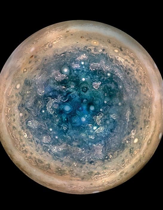
A Juno masterpiece: Jupiter’s south pole covered in cyclones. (Courtesy: NASA / JPL-Caltech / SwRI / MSSS / Betsy Asher Hall / Gervasio Robles)
NASA’s Juno mission has sent back stunning images of Jupiter’s poles. The above image shows the gas-giant’s south pole. The spacecraft’s JunoCam instrument took multiple pictures from an altitude of 52,000 km on three separate orbits, allowing researchers to create full enhanced colour projection. The images of both poles reveal that they are covered in Earth-sized swirling storms up to 1000 km across, but do not look like each other. “We’re questioning whether this is a dynamic system, and are we seeing just one stage, and over the next year, we’re going to watch it disappear, or is this a stable configuration and these storms are circulating around one another?” explains Juno’s principal investigator Scott Bolton. As well as the images, Juno sent back a huge array of results from its first data-collection pass. They are presented in two Science papers and 44 papers in Geophysical Research Letters. “There is so much going on here that we didn’t expect, that we have had to take a step back and begin to rethink this as a whole new Jupiter,” says Bolton.
Small water droplets show unexpected order
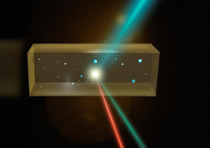
Ordered water: researchers studied tiny water droplets in oil. The method involves overlapping ultrashort laser pulses in a mixture of water droplets in liquid oil and detecting photons that are scattered only from the interface. (Courtesy: EPFL / Julia Jacobi, Laboratory for Fundamental BioPhotonic)
Tiny water drops have surprisingly ordered surfaces, according to Sylvie Roke from École Polytechnique Fédérale de Lausanne (EPFL) in Switzerland and colleagues. The team looked at droplets with a diameter of around 200 nm. Such nanoscale beads of water are everywhere – in the air, rocks, oil fields and even our bodies – and therefore understanding their behaviour may provide insights into atmospheric, geological and biological processes. To study the tiny droplets, the scientists look at how their curved surfaces interact with the surrounding water-repellent environment. “The method involves overlapping ultrashort laser pulses in a mixture of water droplets in liquid oil and detecting photons that are scattered only from the interface,” explains Roke. “These photons have the sum frequency of the incoming photons and are thus of a different colour. With this newly generated colour we can know the structure of only the interface.” The team discovered that the surfaces of these tiny pockets of water at room temperature are much more ordered than that of normal water. The enhanced tetrahedral structure is instead comparable to super-cooled water – liquid water below the freezing point – which has very strong hydrogen bonds between the water molecules. The results, presented in Nature Communications, suggest the nano-droplets may have reduced reactivity, and further studies will investigate how this affects real-world systems.
Study places limit on a “fifth force”
A new way of working out whether a “fifth force” exists has been developed by an international team led by Andrea Ghez and Aurélien Hees at the University of California, Los Angeles. The group looked at the motions of two stars (S0-2 and S0-38), which orbit the supermassive black hole (SMBH) at the centre of the Milky Way. The stars were monitored for 19 years, which is roughly the time it takes the stars to complete an orbit of the SMBH. The team looked for deviations from the trajectories predicted by Einstein’s general theory of relativity, and no discrepancies were seen. This suggests that the strength of a fifth force is less than 1.6% the strength of gravity. Modern physics includes four forces: gravity, and the electromagnetic, strong and weak forces. A hypothetical fifth force appears in some theories that try to unify gravity with quantum mechanics or to explain dark matter and dark energy. While much stronger exclusions of a fifth force have already been obtained by studying forces on masses on Earth and also on objects within the solar system, this is the first study to look at large objects in the huge gravitational field of a SMBH. Writing in Physical Review Letters, Ghez, Hees and colleagues point out that their measurement should be improved next year when one of the stars makes its closest approach to the SMBH, where a deviation from general relatively could be strongest.
Topological magnetoelectric effect rotates light
New twist: topological magnetoelectric effect in action. (Courtesy: Technical University of Vienna)
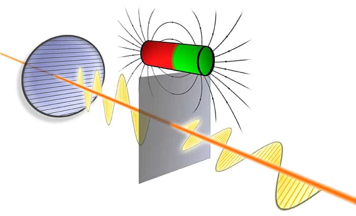
A new interaction between light and a material has been observed by physicists in Austria and Germany. The team shone a polarized beam of terahertz electromagnetic radiation through a thin film that included a topological insulator in an applied magnetic field. The researchers found that the polarization of the beam is rotated by a specific angle as it travels through the material. At first glance, this rotation is similar to the well-known magneto-optical effect that occurs when light passes through a magnetic material. However, Andrei Pimenov and colleagues at the Technical University of Vienna and the University of Würzburg found that the angle is independent of the thickness of the topological insulator – which is not the case for the magneto-optical effect. Furthermore, they found that the angle is fixed at a specific value that is related to the fine-structure constant. This is a dimensionless quantity that defines the strength of the electromagnetic interaction. According to the team, the polarization is rotated by a fixed value every time it passes through a surface of the topological insulator. The researchers say this is related to the peculiar properties of a topological insulator, which is an electrical conductor at its surfaces but an insulator in the bulk. Writing in Nature Communications, the team says that this “topological magnetoelectric effect” could provide a way of defining three basic physical constants that are related to the fine structure constant: the charge of the electron, the speed of light and the Planck constant.
With our persistent march towards nuclear fusion, the need for technologies that can operate in high-energy environments is becoming ever more urgent. Now, researchers in the UK and Spain have discovered a material that can allow us to take pictures inside a nuclear reactor.
In the past, graphene has been used in the design of flexible photodetectors that operate over a large range of frequencies. However, compared to current inorganic photodetectors, the resolution and power response just do not measure up.
Chemical doping of graphene can help some of these problems by increasing the density of charge carriers (electrons or holes). Adding iron-chloride (FeCl3) molecules between a few layers of graphene has been shown to lead to extremely high concentrations of carriers in the material. This FeCl3-intercalated few-layer graphene (FLG) is also stable in ambient conditions. It is 1000 times more conductive than pure single-layer graphene, while retaining an equally low absorption in the visible frequency range.
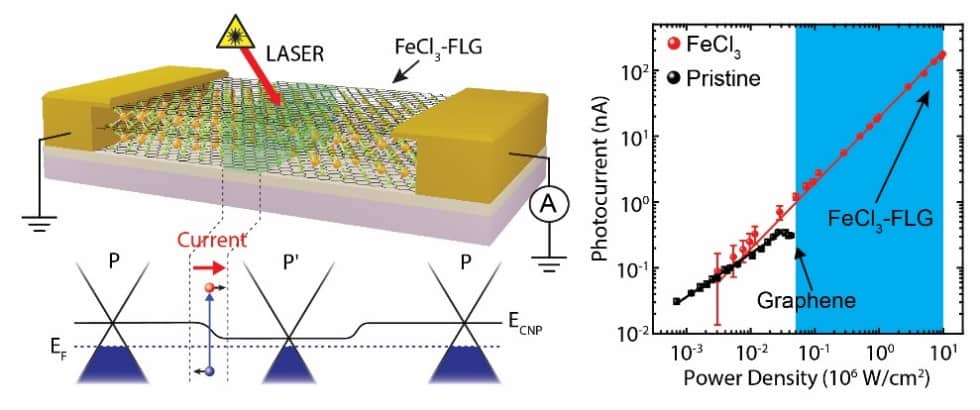
Starting with this material as a base, Saverio Russo and his group at the University of Exeter, UK, used a laser to engrave regions of lower carrier concentration. The laser removes some of the FeCl3 molecules, creating photoactive junctions between highly doped and laser-treated regions of the material. When light shines on this junction, a current is detected across the material, like in a pixel in a camera sensor.
The recipe for extreme photodetectors
The cleverness of this particular material lies in the ultra-high carrier concentration and accelerated cooling of the carriers. Unlike in previously studied devices, the response of the carriers is purely photovoltaic. In FeCl3-intercalated FLG, when the carriers are generated by the incident photons, the electric field created by the difference in charge density on either side of the junction leads to a separation of electrons and holes. This in turn leads to a current.
To the left, a schematic shows the iron-chloride intercalated graphene device. A laser engraves regions of lower doping, creating photoactive junctions between the p p’ p regions, illustrated in the band diagram below. To the right is a plot of the response of the photodetector with power of incident photons. This demonstrated the enhanced linear dynamic range (blue shaded region) of this material (red line) compared to pure graphene (black line). Image courtesy of A De Sanctis.
In other graphene-based photodetectors the carrier behaviour is dominated by the photothermoelectric (PTE) effect; the difference in Seebeck coefficients either side of the junction is responsible for the diffusion of hot carriers when illuminated, as in a common thermocouple. This means the response is spread across an area of a few μm, which limits the size and packing density of the pixels. Using FeCl3-intercalated FLG instead has a huge advantage here, as the miniaturization of pixels is not hindered by a need for thermal isolation.
“This is truly a wonder material; our results show for the first time that graphene-based photodetectors are not always dominated by the PTE,” says Adolfo De Sanctis, lead author of the paper. A reduction of the PTE effect, in fact, results in another marvel. Pixels made from FeCl3-intercalated FLG have a linear (and therefore predictable and reliable) response to photons over a range of incident powers that reaches around 4500 times higher than for other graphene-based devices. This huge linear dynamic range holds true for frequencies from mid-IR to UV-A. This makes these pixels ideal for extreme environments, such as within nuclear reactors, or for working with the high-energy lasers needed for nuclear fusion.
Breaking the diffraction limit
In the absence of the PTE effect, the size of the junctions is instead constrained by the diffraction limit of the laser used to create them. In collaboration with a team at the Institut de Ciències Fotòniques (ICFO), Spain, led by Frank Koppens, the researchers pushed beyond the limits of diffraction when creating the junctions. Using near-field optical nanoscopy, they were able to carve away the FeCl3 molecules and create a junction with a width of only 250 nm, more than halving the diffraction limit of the laser.
The next challenge that faces the researchers lies in producing larger sheets of this exciting material. They can then pattern extensive arrays of photoactive junctions, creating an imaging device suitable for the extreme environments that modern research is leading us towards.
You can read more about this work in the original paper, published in Science Advances.


 By Matin Durrani