Nathan Berkovits has a very simple office. There’s a desk with a computer, a crumpled sofa, a few chairs and a whiteboard covered with equations. But then you don’t really need anything too fancy if you’re a string theorist – apart from an innate mathematical aptitude for describing the fundamental interactions of nature in terms of 1D strings. In fact, the relatively low cost of theoretical physics has always made it a popular choice for emerging nations to kick-start their scientific efforts. Brazil is no exception: the Institute for Theoretical Physics (IFT) at São Paulo State University (UNESP), where Berkovits is based, dates back to 1951, when Brazilian science was just getting off the ground.
But for the past two years, Berkovits has had new things on his mind other than wondering why string theory only holds true in a 10D world or figuring out how to “compactify” the extra dimensions so that it tallies with our familiar 4D world. That’s because in February 2012 he took over as acting head of the first overseas offshoot of the renowned International Centre for Theoretical Physics (ICTP) in Italy. Rather cumbersomely known as the ICTP South American Institute for Fundamental Research, the ICTP-SAIFR has the same aims as its parent institute, which are to carry out top-quality theoretical physics, host scientific schools and workshops, and invite leading scientists to stay.
The ICTP-SAIFR is located on the first floor of the existing six-storey IFT building in the downtown Barra Funda district of São Paulo – the largest city in South America. It may look like many other university buildings, but the institute is remarkable in that it is the physical realization of the ICTP’s founding father Abdus Salam. When he set up the ICTP on Italy’s Adriatic coast in 1964, Salam wanted it to pursue world-class research and nurture scientists in the developing world, which it has done to great effect in the intervening 50 years. But Salam, who died in 1996, also wanted the ICTP to set up regional satellite centres in developing nations.
Salam’s vision was finally realized in 2012 with the founding of ICTP-SAIFR, which receives most of its budget from the São Paulo Research Foundation (FAPESP), with additional support from the ICTP and UNESP. Some 20 UNESP professors are affiliated to the IFT, and the first of a further five permanent faculty members of the new institute – particle theorist Eduardo Pontón from Columbia – has already been recruited. These faculty are being unearthed by a prestigious international search committee featuring star names like string theorist Ed Witten, cosmologist Martin Rees and particle theorist David Gross. “We are interested in experienced people who can come and set up a new group of promising theorists at the start of their careers,” says Berkovits.
International appeal
The ICTP-SAIFR has so far run 10 international schools, eight mini-courses and seven workshops attended by some 1000 visitors. It is also home to nine full-time postdocs, one of whom is Riccardo Sturani, who moved to São Paulo from Italy in March 2013 after his contract at the University of Urbino ended. Sturani models cosmological sources of gravitational waves and calculates what these signals might look like if seen at detectors such as LIGO in the US and VIRGO in Italy. But with no previous connection with the ICTP, Sturani certainly would not be living and working in São Paulo were it not for the new institute. “The institute is very good – it’s active and you can discuss your work a lot,” he says. “The only drawback is that living in São Paulo is very hard for me – I’m not used to big cities and I don’t often get to see my friends back home.”
Despite the loud, noisy, big-city vibe, Sturani admits he would consider staying in São Paulo once his contract is up. In fact, the many charms of the city – including its friendly people and vibrant cultural life – can be hard to resist. Just ask the US-born Berkovits, who studied physics at Harvard University and did a PhD at the University of California, Berkeley before moving to Brazil in the mid-1990s. Back then, many home-grown Brazilian physicists still opted to further their careers by working abroad, so going in the opposite direction might have seemed an odd move for a young researcher. “Actually, I saw it as a challenge,” he recalls. “It felt like something new for me, plus I like Brazil and it’s enjoyable living here. People are optimistic, friendly and helpful, and see the country getting better.”
But one thing that has not changed in the 20 years since Berkovits first came to Brazil is that it is still a highly bureaucratic nation. Dealing with paperwork can be infuriating and time-consuming for university researchers, reducing their time for science. The bureaucracy can also mean that people get selected for academic posts for reasons that are not always transparent. But with its unique form of funding, the ICTP-SAIFR can “get round” the system, for example by letting Berkovits recruit scientists in a clear and rigorous way. And in a relatively conservative nation where there is a wide resistance to change, the presence of a new, outward-looking institute can only be a good thing for Brazil.
The technique of 3D printing, more accurately known as additive manufacturing, has enjoyed extensive coverage in the media in recent years. Consumers will play an increasing role in manufacturing the products they use regularly, it is often suggested, perhaps even designing those products themselves. One frequently cited scenario involves consumers using free Web-based packages or mobile-phone photogrammetry applications to specify a design, then submitting it to a commercial 3D-printer operator who will carry out the manufacturing step and ship the product directly to them.
To a limited extent, this picture is already a reality. The commercial availability of low-cost 3D printers over the past five years has certainly allowed consumers to operate home-based manufacturing technology. Such low-cost platforms, which have come about because of the expiry of patents covering earlier prototyping systems, work on a principle called “filament extrusion”, in which a thin polymer thread held at a temperature close to its melting point is squeezed out from a small hole and deposited in raster fashion on a substrate. Consumers are also beginning to take advantage of commercial 3D-printing services, which use established industrial laser-based systems that generally work on the “powder bed” principle: a high-power laser scanned across an extremely thin bed of powder fuses a slice of a 3D object together, and the process is repeated to build up a volume.
Consumer devices bear little resemblance to their industrial additive-manufacturing counterparts, however. They tend to be able to deal only with a handful of extruded thermoplastic materials and – despite the “you can make anything” hype – are greatly limited in the size, resolution and complexity of the parts that they can produce. Indeed, low-cost 3D printing makes up only a relatively small part of the overall 3D-printing industry: around 6% by revenue.
At the more established industrial end of the spectrum, however, the variety of printable material types has increased to include polymers, metals and ceramics. Such single-material addition is already an established manufacturing process in many sectors, including the hearing-aid industry, which manufactures millions of custom hearing-aid shells annually using stereolithography. Selective laser-melting technology has also recently been adopted by GE Avionics to produce metallic components in aero engines, while polymer laser-sintering technology is allowing firms such as FreshFiber to produce customized and complex designs for smartphone covers.
Researchers are now exploring 3D-printing techniques that not only allow complex objects to be manufactured at low cost from almost any material, but will also enable objects with different functionalities to be printed in a single step. This next generation of additive-manufacturing technologies, which is rooted in advanced material-deposition systems and optical techniques, is being investigated by the Engineering and Physical Sciences Research Council’s Centre for Innovative Manufacturing in Additive Manufacturing at the University of Nottingham in the UK, which is undertaking internationally leading work in multifunctional 3D-printing research.
Beyond the hype
It might seem that 3D printing is a novel technology. In fact, the underlying principle – in which raw material is deposited layer by layer without the need for moulds, tools or dies – was first commercialized almost three decades ago. Originally developed for rapid design studies and prototyping, the earliest 3D-printing systems used an ultraviolet laser to selectively photopolymerize a liquid photocurable monomer resin, repeating the process layer by layer until the part is completed. Successive innovations since then have led to the spectrum of additive systems we know today, including the low-cost extrusion-based machines as well as industrial systems based on fusing powders using infrared lasers.
As one of the leading research groups in this area, the 3D Printing Research Group at Nottingham is going beyond single-material 3D printing. Rather than incrementally improving existing single-material approaches, we are working on the next generation of systems capable of depositing multiple materials all at once. Doing so will enable the technology to leap beyond simple structural applications and allow the delivery of entire functionalized systems, such as 3D circuitry, drug-delivery systems and even biological tissue, within a single processing step.
We expect that multifunctional 3D printing will be commercially available within the next 15 years, but there are major technical challenges ahead
We expect that multifunctional 3D printing will be commercially available within the next 15 years, but there are major technical challenges ahead. These range from the accurate and reliable simultaneous deposition of different materials to the design of components and how best to integrate different materials for a given function. The variety of disciplines involved reflects the vastly different functional properties that could be printed directly into structural products: electrical circuitry, optical tracks, embedded sensors, energy sources, displays, antennas, chemical agents and even biologically active structures are just some of the many targets. A large part of research in this area is therefore focused on the search for functional 3D-printing materials.
New design approach
The first challenge, however, is to create a design methodology that enables us to integrate printed structures with lattices that contain functional components. Constraints within traditional manufacturing approaches, such as injection moulding or CNC machining, mean that, in general, it is not possible to fabricate the optimal shape for a given task. Instead, we are turning to algorithms that seek out the optimal shape or composition for a device taking into account weight, aesthetics and functionality in a single processing step.
A promising technique for depositing structural materials, especially engineering polymers, is drop-on-demand ink-jetting. This can take two forms: directly jetting a material that is suspended or in solution; and “reactive jetting”, whereby a monomer and catalyst are deposited separately and polymerization occurs in situ during the manufacturing process. This minimizes waste, reduces the need for solvents and opens up a wider range of materials that can be printed. Our group has printed nylon using this approach, but the current focus is on engineering materials that include polymethyl methacrylate, polyimides and polyurethane.
We are also investigating materials and deposition processes for conductive and dielectric systems, including highly novel research into the ink-jetting of metals with a melt temperature up to 1500 °C. This work, to be carried out in collaboration with the Netherlands-based manufacturer Océ, can potentially overcome limitations with conventional printed-electronics materials (such as their low conductivities), which currently rely on inks that have been loaded with nanoparticles of active materials such as silver.
One of the most exciting developments in this field is the creation of multifunctional structures at the nanoscale, which demands further improvements in the deposition resolution. At Nottingham we are developing a multi-photon lithography system that can produce arbitrary 3D structures of the order of 100 nm for advanced micro- or nanoscale applications, and using optical-tweezer technology to functionalize the structures deposited (see box). By coupling these two systems we can open the door to new nanoscale devices and structures, for example by providing the sensory input for embedded data-processing capability.
Dial-up medicine
Over the coming years multifunctional 3D printing will move beyond fundamental research towards new manufacturing systems. Currently, we are at the stage of understanding the fundamental principles and challenges of multifunctional 3D printing, but it is clear that we need a joined-up approach between numerous disciplines – including physics, chemistry, optics, electronics, materials science, biology and pharmaceutics. To this end, we are working with the School of Pharmacy at Nottingham to explore the 3D printing of pills and multiple therapeutics designed to release drugs at a rate that is personalized to the patient. This would lead to a radically decentralized business model in which drugs or implants could be distributively manufactured. It is envisaged that a medical practitioner would be able to “dial up” a treatment that is then made to a bespoke specification in a room next door, offering personalized care to patients at the point of need.
Multifunctional 3D printing promises genuinely new kinds of manufacturing processes with advanced capabilities, and ultimately a new generation of optimized and highly functional products. Supported by innovative business models, these products will set new standards in performance, efficiency and user-friendliness.
Optical techniques carve nanoscale features
Printing functional nanoscale devices calls for sophisticated optical techniques. Two-photon polymerization (left) allows a finer resolution than is possible with more common single-photon absorption methods. By using photons with half the energy required to drive a polymerization reaction, the two photons need to be absorbed within a very short timescale. Because this process is proportional to the square of the intensity of photons incident on the target, only in the most focused regions of the incident light – when using a high numerical aperture and a femtosecond-pulsed laser – will two-photon absorption occur, therefore resulting in high resolution and feature sizes of the order of 100 nm. By coupling this set-up with an optical-tweezer arrangement, whereby very small forces can be exerted on an object through the focusing of a laser beam (right), larger micron-sized objects can be drawn into the vat of material and encased within a matrix or attached to a surface. This offers the potential for functionalizing a surface or a material by combining it with particles prepared separately and then brought together.
During the Second World War, the US military developed a method to distinguish real plants from enemy camouflage based on the way they react to light. Chlorophyll absorbs blue and red light while reflecting green, giving plants their colour. But plant cells also reflect infrared light, which is not energetic enough for photosynthesis, to prevent overheating. Therefore, while green camouflage looks the same colour as a plant to the naked eye, it appears dark on an infrared film, while vegetation appears white.
As remote sensing from satellites became possible in the 1960s, this principle was developed into an index called the normalized difference vegetation index (NDVI), which relates reflectance in the visible region to the infrared. The NDVI also provides a measure of how healthy a plant is based on its photosynthetic activity: an increase in the reflectance of red light indicates that a plant is not photosynthesizing as effectively as usual, perhaps because of drought or lack of nutrients. However, satellite NDVI measurements are also affected by atmospheric conditions, satellite geometry and the angle of incidence of the Sun’s radiation.
Gauging a plant’s needs
To get round these complications, in the 1990s plant scientists and agricultural engineers at Oklahoma State University in the US developed ground-based optical sensors. Their aim was to use NDVI measurements to gauge a plant’s nitrogen needs, thereby allowing farmers to adjust the amount of fertilizer applied to a crop. Early sensors were passive and worked by measuring light reflected from the Sun, which varies during the course of a day and with the level of cloud cover. In 1998, however, researchers developed active sensors using LEDs as a red and infrared source, and by 2002 US firm NTech Industries had commercialized the technology under the trademark “GreenSeeker”.
Big business
Crop sensing has expanded rapidly in the last few years, with the acquisition of NTech by Californian firm Trimble in 2009 and the appearance of competitors such as Holland Scientific’s Crop Circle and Topcon’s CropSpec, which uses a laser diode rather than an LED source. In today’s systems, several sensors are mounted along a boom attached to a tractor and readings are used to adjust the levels of fertilizer being applied in real time. A typical four-sensor GreenSeeker system costs in the region of $10,000, but the resulting savings can be much bigger according to Trimble’s Anna Hebert. “A farmer in Oklahoma saved more than $32,000 in fertilizer costs in 2013 ($24 per acre) and more than $175,000 since he began using GreenSeeker in 2005,” she says.
The next move for agricultural optics appears to be upwards. Andreas Burkart at the Jülich Research Centre in Germany is leading a project to observe crops using a lightweight spectrometer made by US firm Ocean Optics aboard an unmanned aerial vehicle (UAV). “The dream of such an ‘eye in the sky’ is old,” says Burkart, “but now UAVs can be readily purchased and configured so that even a biologist like me can operate one easily.” The restricted payloads and flight times of UAVs make such systems more suitable for crop observation than treatment. Indeed, according to Michael Allen of Ocean Optics, the UAV device captures data about 20 times faster than with traditional ground-based techniques without causing any disturbance to the crops. “That’s a huge advantage when you have to assess dozens of acres of cropland,” Allen told Physics World.
The next step, says the Jülich team, is to use spectral data to reconstruct a full phenotype, including the size of plants, and the number and colour of their leaves. A UAV could then quickly scan an area containing several different varieties of a crop, such as barley, and assess how each performs in different conditions. Trimble launched its first UAV system targeted at farmers in January.
Unlike ground-based active optical sensors, measurements from the air rely on reflected light. But a recent project by a multidisciplinary group at the University of New England in Australia aims to get the best of both worlds by mounting off-the-shelf active optical sensors on ultra-low-level aircraft flying 3–5 m above the ground.
Detecting disease
Researchers are also developing more advanced sensors. For example, the small amount of red light re-emitted after being absorbed in photosynthesis, known as chlorophyll fluorescence, can provide a sensitive indicator of plant stress. Optical techniques have even been demonstrated that can detect plant diseases before they can be ascertained any other way, allowing the preventative application of pesticides. By studying the reflectance spectra of sugar-beet crops infected with three different fungal pathogens, a team from the Institute for Crop Science and Resource Conservation at the University of Bonn in Germany has recently identified spectral features that are correlated with each disease.
“From online measurements of the fat content of milk to screening incoming materials for food manufacturing, optical solutions are becoming mainstream,” says Allen. “Miniaturization and ease of use will drive more farmers to optical technologies.”
A modern laptop is 100 times smaller, a million times faster and 10,000 times less expensive than the first general-purpose electronic computer built in 1946. This remarkable reduction in size and cost is largely down to semiconductor-fabrication methods that have been developed since the 1960s, which allow large and complex electrical circuits to be miniaturized onto tiny chips. But the technology is by no means limited to computers – the modern solid-state laser has benefited from a similar trend.
By combining state-of-the-art nanofabrication techniques with modern photonics and solid-state lasers, researchers are attempting to shrink some of the largest scientific instruments ever built: particle accelerators. This could lead to a new generation of compact and affordable machines for high-energy-physics exploration and X-ray science, and industrial devices for cancer therapy, food sterilization and security.
Conventional particle accelerators confine microwave energy in specially designed hollow metallic guides called radio-frequency cavities, which deliver a forward thrust to particles passing through them. As the microwave power is increased, the particles gain more energy. However, as is clear to anyone who has put a metallic object inside a microwave oven, the interior metal surfaces of a cavity begin to suffer electrical breakdown if the microwave power gets too high. This phenomenon leads to electrical arcs that can damage the machine, and limits the amount of energy that particles can gain over a given distance – a quantity called the accelerating gradient – to around 30 MeV/m. The only way to increase the energy of conventional accelerators is therefore to make them bigger.
In a research collaboration based at Stanford University and the SLAC National Accelerator Laboratory in California, US, we are using techniques from the microchip industry to make micron-scale accelerator structures from dielectric materials, which have high laser-damage thresholds and low ohmic losses. By accelerating particles using the energy from lasers instead of microwaves, gradients of billions of electron-volts per metre are possible. In principle, this would allow us to shrink conventional accelerators by a factor of 100 or more for a given particle energy.
The idea of using light to accelerate particles dates back to the 1960s, and since then a variety of all-dielectric, high-gradient structures have been proposed. But it is only recently that it became possible to fabricate the first laser-accelerator prototypes, thanks to high-power solid-state lasers, optical fibres and photolithographic techniques driven by the communications and semiconductor industries.
An alternative approach that has made impressive strides in recent years is plasma acceleration. When an ionized gas (or plasma) is excited by an intense laser pulse, it produces a wave that accelerates a trailing bunch of particles – similar to a surfer riding on the wake of a motorboat. Plasma accelerators use intense lasers that provide millions of billions of watts of peak power to excite the plasma wave, with one excitation occurring every few seconds.
By comparison, photonic-microstructure-based accelerators would use off-the-shelf tabletop lasers to produce millions of pulses per second with a high energy efficiency. This large number of pulses potentially allows micro-accelerators to operate with beam currents comparable to those in conventional accelerators, despite their tiny size, and such devices could also be mass-produced inexpensively.
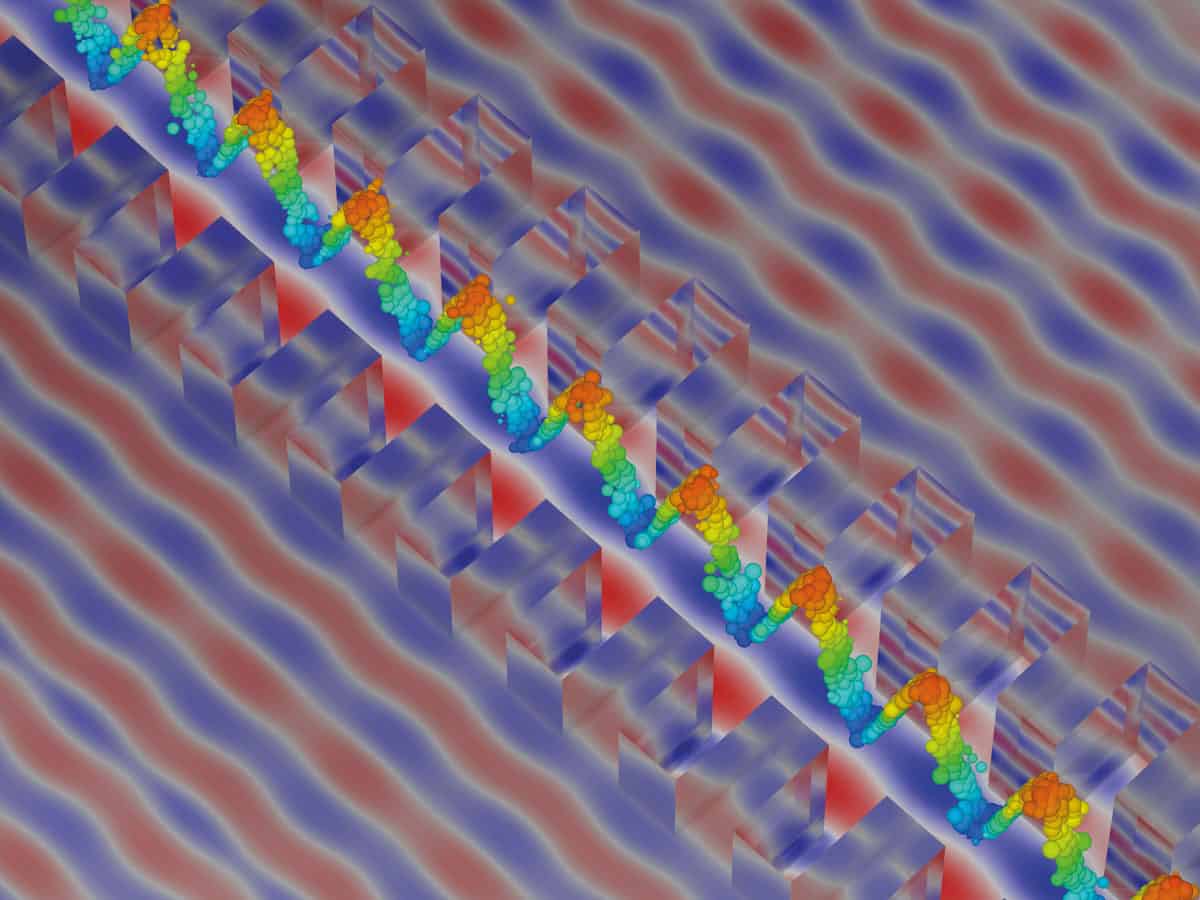
The first demonstrations of chip-based photonic accelerators were carried out by the SLAC–Stanford collaboration in 2013. Graduate students Edgar Peralta and Ken Soong, respectively, fabricated the prototype structures and developed the precision laser optics required to test them. Using photolithography, more than 200 individual accelerators were etched into a pair of bonded silica wafers. Each of the 1 mm2 devices contains a channel as narrow as 400 nm, into which are etched a sequence of ridges and gaps. When illuminated by a laser, these ridges shape the laser field to produce a wave that can impart energy to a particle that arrives at the appropriate time (see figure below).
Because most applications require particle accelerators to operate at relativistic energies, we designed the micro-accelerators to produce a wave that will continuously accelerate particles travelling at near-light speeds. To demonstrate the effect, individual structures were carefully aligned in the path of a pre-accelerated electron test beam at SLAC, while being illuminated by a titanium-sapphire laser. Because the particles arrived in bunches that were longer than the 800 nm wavelength of the laser, some were accelerated and some decelerated depending on whether they arrived at the peak or at the trough of the accelerating wave.
Surfing a wave A computer simulation of particles in a microchip accelerator shows the accelerating (orange) and decelerating (blue) portions of the laser-induced wave in a nanostructured channel. (Courtesy: Ben Cowan, Tech-X Corp.)
High gradients
Our initial tests last year demonstrated accelerating gradients as high as 300 MeV/m (Nature503 91), but by further narrowing the width of the accelerating channel to enhance the accelerating field and using materials such as sapphire that can withstand higher laser intensities, it should be possible to increase the gradient by a factor of 10 or more. This would allow us, in principle, to shrink the entire 3 km-long SLAC linear accelerator to the size of a room, or to create lower-energy medical accelerators on a single wafer that would fit in your hand.
Alongside our ongoing experimental efforts, Peter Hommelhoff at Friedrich Alexander University in Germany and co-workers recently used an approach similar to ours to accelerate lower-energy (28 keV) electrons with gradients of 25 MeV/m (Phys. Rev. Lett.111 134803). The German group is also developing ways to fabricate sub-micron-sized particle sources that can be triggered using the same laser that powers the accelerators. Such a particle injector would negate the need for a conventional radio-frequency accelerator on the front end of the microchip accelerator, as was necessary in our experiments, and is vital for making on-chip devices that can accelerate electrons to sufficiently high energies.
These first demonstrations of chip-scale accelerators are important steps, but a complete accelerator is still some way off. To reach useful particle energies, many of these tiny structures must be fabricated in succession and illuminated by a sequence of laser pulses that are precisely timed so that the particles see a continuous energy gain as they travel forward. The arrival times of the electrons and the laser must be synchronized to within a fraction of an optical period, corresponding to a few tens of attoseconds. This could be done, for instance, by introducing on-chip light guides with precise lengths that selectively funnel light into successive structures.
Another challenge is to avoid some of the particles being decelerated instead of accelerated. This requires that the incoming particles arrive in bunches that are separated by a distance equal to the wavelength of the laser and timed so that they all ride on the peak of the accelerating wave. Researchers at SLAC and Stanford have previously demonstrated a way to prepare the particles in this way using a laser to modulate the energy of the electrons followed by a magnetic compressor, which allows lower-energy particles to catch up with higher-energy ones. Accelerating these micro-bunched particles in unison at the peak accelerating field would also allow for monochromatic beams with a narrow energy spread, and we are now trying to integrate these approaches to design new particle sources that are optimized for testing micro-accelerators.
Similar techniques have been proposed to build a powerful source of pulsed X-rays for advanced crystallography research, for instance. By making on-chip laser-driven devices rapidly deflect rather than accelerate particles, a sequence of alternating deflectors in series would form an “undulator” that forces electrons to wiggle back and forth to generate bursts of synchrotron radiation. Such micro-bunched beams could potentially deliver X-ray pulses with durations of tens of attoseconds, allowing scientists to probe atomic and molecular dynamics on timescales three to four orders of magnitude shorter than present-day “conventional” X-ray free-electron lasers, such as the Linac Coherent Light Source at SLAC.
Industry appeal
We estimate that within the next 5–10 years tens of millions of electron-volts could be generated in an integrated device fabricated on a single 15 cm diameter wafer. To reach the billions or trillions of electron-volts needed for high-energy physics exploration, we will need to carefully align many such wafers in succession with sub-micron precision. This is straightforward when nanofabricating multiple devices on a single wafer, but more challenging if individual macroscopic objects are to be aligned. Consequently, in the next decade microchip accelerators will probably find their first applications in industry and medicine, where the required particle energies are in the much lower range of 1–20 MeV.
Companies that build accelerators for these sectors are beginning to express interest in commercializing the technology. Although the machines used in industry and medicine are smaller than high-energy colliders, they can still be the size of a room, weigh tens of tonnes and cost millions of dollars. Microchip-based versions could be sufficiently small and portable to allow endoscopic direct electron-beam cancer therapy, for instance. They could also enable more affordable medical X-ray sources for the treatment of clogged arteries, computed tomography (CT) scans and high-resolution imaging of biological tissues.
Similar devices for industry could provide a valuable X-ray source for non-destructive testing of products and materials, for instance by identifying cracks and deformations in hard-to-reach locations, or enabling new processes in the microchip industry by using multiple-beam X-ray lithography to rapidly “print” nanoscale patterns onto integrated chips. Accelerators for X-ray security screening of cargo and aircraft could also be made more widely available and, being smaller, capable of scanning larger areas or moving targets.
A number of these nearer-term applications are beginning to be explored and although the technology is not yet ready to compete with high-energy machines such as the 27 km-circumference Large Hadron Collider at CERN in Switzerland, it is clear that photonic devices are a promising approach for the future of particle acceleration.
Illustration showing how a single laser beam is converted into four beams after diffracting from a patterned surface. These beams are then used to trap ultracold atoms in the new accelerometer. (Courtesy: National Physical Laboratory)
Physicists in the UK are developing an accelerometer for the Royal Navy, based on the quantum interference of ultracold atoms. The device will allow submarines to pinpoint their position underwater to within 1 m after travelling one day, without having to surface to use GPS. This is much better than is possible with current accelerometers, which are accurate to within 1 km after a day’s travel. With further development, the device could be used for oil exploration or even to do “gravity scans” of concealed objects.
Since the 1990s, physicists have been able to do interferometry experiments with ultracold atoms. Pioneered by Stanford University’s Mark Kasevich, the classic version of the experiment involves allowing an atom to fall under the influence of the Earth’s gravity. A laser pulse is fired at the atom that puts it in a superposition of two quantum states, which follow different trajectories much like photons travelling through an optical interferometer. A second pulse recombines the states and the resulting interference gives a precise measure of gravity – and can even reveal subtle effects of the general theory of relativity.
Extremely sensitive
Such a device can also be used as an extremely sensitive vertical accelerometer. Now, Ed Hinds and colleagues at Imperial College London have taken this experiment and rotated it by 90° to make an accelerometer that works in the horizontal direction. The device uses about one million rubidium atoms, which are trapped on an integrated chip using a magnetic field and laser light.
An important feature of the chip is that a single beam of laser light is used to trap the atoms. This beam is fired at a surface grating to create several beams of diffracted light, which together with a magnetic field are then used to trap the atoms.
The atoms have two quantum ground states, which the researchers denote as |1〉 and |2〉. The system is prepared so that all of the atoms are in |1〉 and then a light pulse puts the atoms into a superposition of |1〉 and |2〉. This action plays the role of the first beamsplitter in an optical Sagnac interferometer. State |1〉 has no recoil, while state |2〉 recoils along the direction defined by the light beams. Then, a second light pulse is fired at the atoms and this swaps the states so that |1〉 (with no recoil) becomes |2〉 (with recoil) and vice versa. This is analogous to the two mirrors of an optical interferometer, which direct the two diverging light beams towards a second beamsplitter, where they are recombined. Finally, a third light pulse plays the same role as the second beamsplitter of an optical interferometer.
Taking different paths
A measurement is then made to determine how many of the atoms are in state |1〉 – or, alternatively, how many are in |2〉. Either measurement can be used to compute the interferometer phase, which is related to the effective path difference taken by the two states. This path difference is proportional to the acceleration of the atoms along the direction of the light beams.
The simple design and operation of the accelerometer means that, in principle, it could be miniaturized for use on submarines. Indeed, the chamber in which the atoms are held has already been miniaturized on a chip. However, the associated electronic and optical components are still mounted in racks and on an optical table. Another challenge is to make the chip impervious to helium gas, which can leak through the walls and eventually contaminate the vacuum in which the atoms must be held.
Gravity scanners
The team is now working on shrinking the optical and electronic components of the accelerometer so that it can fit into about 1 m3. While this would make it suitable for naval use, the device would have to be further miniaturized – to the size of a beer can, for instance – before it could be sent down an exploratory bore hole to search for oil or other mineral deposits. Other possible applications that could emerge in a 5–10-year timeframe include “gravity scanners” that can peer into sealed containers and create density maps of their contents.
Hinds told physicsworld.com that it is likely that similar devices are being created for the navies of other nations. Indeed, Kasevich and colleagues have unveiled an atomic-interferometry-based “quantum gyroscope”, which is essentially an accelerometer that can be used for navigation. At the time, Kasevich said that the technology was going to be commercialized by AOsense, a company that he co-founded (see “Falling atoms measure the Earth’s rotation”).
The chip used by Hinds to trap the rubidium atoms is described in Nature Nanotechnology.
General relativity put to the test
In another recent development in the field, physicists in Germany and the US have used atomic interferometry to measure the effects of gravity on two different atoms: rubidium and potassium. The experiment found that the acceleration due to gravity experienced by both types of atoms is the same to one part in 10 million. This is the latest verification of the universality of free fall, which is a cornerstone of Einstein’s general theory of relativity. The rubidium atoms are more than twice as massive as their potassium counterparts. If they were seen to respond differently to gravity, it could point physicists towards a quantum-mechanical theory of gravity.
The research on the universality of free fall was done by Ernst Rasel of the Leibniz University Hannover, and colleagues, and is reported in Physical Review Letters.
High-energy particle physicists in the US must build further international collaborations and co-operation, according to recommendations made by the Particle Physics Project Prioritization Panel’s (P5) 2014 report, which was released yesterday. Top priorities over the next two decades include the US playing a vital role in upgrades to the Large Hadron Collider (LHC) at CERN in Switzerland and building a long-baseline neutrino facility based at Fermilab near Chicago. The report also calls for US participation in the planned International Linear Collider (ILC), should the project commence. In light of declining funding and tightened budgets for particle physics, the report presents a strategy that would allow the US to “invest purposefully in areas that have the biggest impacts and that make most efficient use of limited resources”.
P5 is part of the US Department of Energy’s High Energy Physics Advisory Panel (HEPAP). Since P5 presented its last report in 2008, the face of high-energy particle physics has changed and evolved, especially in light of the discovery of the Higgs boson particle at CERN.
Main drivers
The 25-member panel began its deliberations in September 2013 following a year-long, community-wide study known as “Snowmass”. Snowmass identified 11 groups of particle-physics questions that could be addressed, and P5 then whittled them down to create the five “drivers” that the panel feel show great promise for discovery in the next two decades.
The drivers are to use the Higgs boson as a new tool for discovery; to pursue the physics associated with neutrino mass; to identify dark matter; to lay the foundations for understanding dark energy and inflation; and finally, to “explore the unknown”, including the study of new particles. While the five “intertwined” drivers themselves were not prioritized in the report, the specific projects are categorized by construction costs as large (>$200M), medium ($50M–$200M) and small (<$50M), as well as a sequential list of large projects.
The list begins with the proposed “muon-to-electron-conversion experiment” or the Mu2e experiment at Fermilab and upgrades to the LHC. Following that is the wish for the US to host an international programme of neutrino research “that will attract the worldwide neutrino community, operating the world’s most powerful neutrino beam and, with international partners, building a major long-baseline neutrino facility complemented by multiple small, short-baseline neutrino experiments”. The panel has recommended that the current “Long-Baseline Neutrino Experiment” (LBNE) be redesigned as an internationally co-ordinated and funded programme called the Long-Baseline Neutrino Facility (LBNF). The report refers to LBNF as “the highest-priority large project in its timeframe”.
The P5 also suggests US participation in the development of an ILC in Japan, specifying that the US “should engage in modest and appropriate levels of ILC accelerator and detector design in areas where the US can contribute critical expertise”.
Varying scenarios
The report’s strategy also considers three different budgetary scenarios – if funding is constant for three years and then increases by 3% per year; if it is constant for three years and then increases by 2% per year; and finally, if funding is unconstrained. They also recommend investing a larger portion of the DOE’s high-energy physics budget in the construction of new experimental facilities, raising it from 16% to 25%.
The panel is quick to point out that the lowest budget scenario they outline is “precarious” and would be “close to the point beyond which the US would not be capable of hosting a large project while maintaining the other core program components”, and that this would, in turn, make the US “lose its position as a global leader in this field, and highly productive international relationships would be fundamentally altered”.
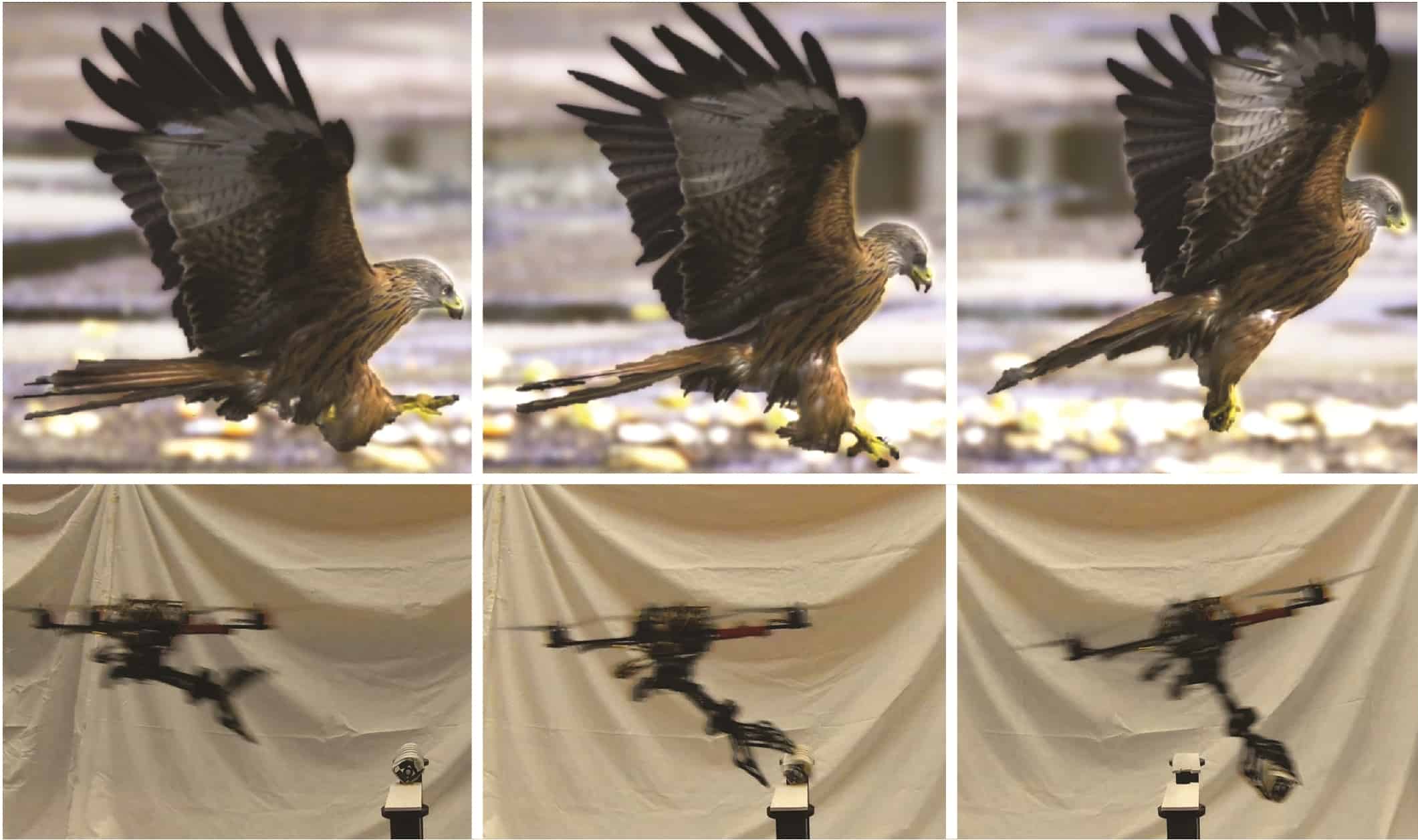
A red kite and a drone swoop down on their prey. (Courtesy: Vijay Kumar)
A bird of prey swoops out of the sky, grabs its victim from the ground and flies off into the distance. It’s what a bird does instinctively, but how could we get a drone aircraft to do the same thing? That’s the subject of one of the papers in a special issue of the journal Bioinspiration & Biomimetics that focuses on “Bioinspired flight control”.
The above sequence of images is from a paper entitled “Toward autonomous avian-inspired grasping for micro aerial vehicles” by Vijay Kumar and colleagues at the University of Pennsylvania. The special issue also includes work on aircraft inspired by flying snakes, flocking birds and incredibly stable moths.
The podcast provides a history of Jodrell Bank, explaining how the observatory was created in 1945 using the radar technologies and expertise developed during the Second World War. The observatory was founded by Bernard Lovell, whose primary goal was to detect cosmic rays, though this initial aim never come to pass. Jodrell Bank’s associate director Tim O’Brien looks back on these early years and how the enthusiasm of the first Jodrell astronomers led to them to commission what would be the world’s largest radio telescope – a giant steerable dish, 250 feet in diameter, now named the Lovell Telescope.
Having moved away from the military applications of radar technology to refocus on fundamental science, Lovell and his colleagues were soon drawn back in as the Cold War escalated. In 1957 the British government asked whether Jodrell Bank’s new giant radio dish could be used to track the rocket used to launch Sputnik I, the world’s first artificial satellite. The fear at the time was that the Soviets would use the same rocket technology to fire an intercontinental ballistic missile at the West. For a brief period in the early 1960s, Jodrell Bank was placed on stand-by to look out for such a dire eventuality, given that it was the only location in the West that could accurately track the missile.
Bernard Lovell (right) in the control room at Jodrell Bank Observatory. When it was constructed in the 1950s, the telescope in this image (now named the Lovell Telescope) was the largest radio telescope in the world – a giant steerable dish some 250 feet in diameter. It played a role in tracking several major missions during the Space Race. (Courtesy: Jodrell Bank Observatory)
Dacey also meets a former director of Jodrell Bank, Francis Graham-Smith, who describes how the observatory teamed up with the Daily Express newspaper in 1966 as the two organizations collaborated to interpret a mysterious signal being beamed back to Earth by the Soviet mission Lunar 9. To find out how this unlikely pairing came about and what it discovered, give the podcast a listen.
A simple way of creating and controlling surface plasmon polaritons (SPPs) in graphene has been demonstrated by researchers in Spain and Argentina. SPPs are quasiparticles that are a hybrid of light and electrons, and the new technique involves using simple gold antennas to channel light energy into the material. The research could lead to the development of new electronic devices that use light.
SPPs are quasiparticles that are combined oscillations of photons and mobile charge carriers, such as electrons. Although they can be excited in metals, they propagate much further in graphene, so several groups are studying the potential of graphene plasmonics as an interface between optical and electronic circuits and devices. One important benefit of SPPs is that their wavelengths are much shorter than visible light, which means that devices based on SPPs can be made much smaller than those based on light. However, there is also a downside: the wavelength of a plasmon in doped graphene is much shorter than that of an incident photon of the same frequency, making the SPP’s momentum much larger. For an incident photon to excite a plasmon in bare graphene would, therefore, violate Newton’s third law, which requires momentum to be conserved.
Channelling momentum
In 2012 researchers in Spain led by Rainer Hillenbrand at CIC nanoGUNE in Donostia-San Sebastian and Frank Koppens at the Institute for Photonic Sciences in Barcelona, in parallel with an independent group in the US, created and imaged SPPs in graphene using a near-field optical microscope. They achieved this using near-field (or evanescent) light, which extends only a very short distance from a surface but can carry very high momentum. By bringing the tip of the microscope – which is a source of evanescent light – very close to the graphene, the researchers could channel much more momentum to the graphene than would otherwise have been possible. Using the same microscope tip, they also imaged reflected SPPs and recorded interference patterns.
Now the Spanish group has found a simpler, more practicable way to excite and control graphene plasmons, which could be useful for future engineering applications. The researchers covered the graphene with tiny gold antennas (bars about 3 μm long) that absorb photons at a particular frequency. This creates an optical dipole in the antenna that, in turn, creates evanescent light. As the antenna is in direct contact with the graphene, energy from the near field creates SPPs in the graphene. By changing the size of the antenna, the frequency of light absorbed can be altered. This changes the frequency of the SPPs that are produced.
Focus and diffraction
The researchers manipulated the SPPs in various ways. For example, a straight antenna launched planar SPP waves, but the team also managed to focus SPPs to a point by using an antenna with a concave tip. They also demonstrated refraction of the SPPs using a 2D “prism” of bilayer graphene. The bilayer graphene has higher electrical conductivity than the monolayer graphene, so the wavelength lengthens inside the prism and the SPPs bend away from the normal according to Snell’s law. In the future, the researchers believe the bilayer should not be necessary. “One could simply apply a gate voltage on a small area of the graphene,” explains Hillenbrand, “and then one could actually tune the wavelength inside the prism to control the refraction angle. That is nearly impossible to do with other materials.” If this could be achieved, it would open the way for a plasmonic transistor, in which a gate voltage could switch a plasmon current on and off.
Before such manipulations can be achieved, however, the team needs to improve the distance SPPs can propagate through the graphene, which at present is limited to 1–2 μm. The researchers are now working to boost the SPP’s range by using higher-quality graphene and looking for ways to dope it more highly, so it has more free electrons. “If one has achieved that,” says Hillenbrand, “I could imagine that these waves should propagate at least one order of magnitude further.”
Graphene expert
Alexander Grigorenko at the University of Manchester says that the work is not only a significant scientific achievement in the degree of control that the researchers have achieved over the graphene SPPs, but also a major technological one in the precision with which they have observed them using a new type of near-field microscope. “I would say there are just two labs in the world that could do something like what they’ve done right now,” he says. “If you talk about long-term importance: who knows?”
In mid-September 2001 letters containing deadly anthrax spores were mailed to several news agencies and two US senators in a terrorist attack that killed five people and injured more than a dozen others. A top-level adviser to president George Bush asked his then science adviser John H Marburger III how to neutralize the spores on existing anthrax-ridden mail. Marburger convened a team of scientists, who came up with a carefully researched recommendation based on irradiating the mail with electron beams. It seemed to be a triumph of science’s application to the American national interest.
But when US Postal Service officials implemented the method – to kill anthrax but preserve the mail – the electron beam burnt some batches to a crisp. Surprised, Marburger investigated. He found that government officials had second-guessed the scientists. The officials had reasoned: if scientists said the right radiation dose to blitz the death spores was x, then 2x was surely safer! When Marburger ordered the dose scaled back, the method worked fine.
Marburger, who died in 2011, liked to cite this episode as a “relatively benign example of a potentially disastrous behaviour”, namely, the tendency of government officials to alter or ignore scientific advice. His store of more damaging examples included the Bush administration’s claim, in 2002, that aluminium tubes sought by Iraq were for a nuclear-weapons programme, contrary to the conclusion of scientists. In these and other cases, it is simply a fact that, as Marburger put it, “the methods of science [are] weaker than other forces in determining the course of action”.
Marburger – the longest-serving US presidential science adviser and an experienced scientist – grew curious about why science has such weak authority among political leaders. After he stepped down in 2009, he began to investigate.
Three grounds for authority
Marburger turned to the works of German historian and sociologist Max Weber, who in his influential book Economy and Society (1922) examined different types of authority, or the grounds on which people voluntarily comply with commands issued by others. There are three, Weber said: traditional, rational-legal and charismatic.
Traditional authority, Weber wrote, is rooted in a “belief in the sanctity of age-old rules and powers”. This is the authority possessed by village elders. Legal authority – the authority of a bureaucracy – is grounded in a “belief in the legality of enacted rules and the right of those elevated to authority under such rules to issue commands”. Charismatic authority is possessed by those who are “considered extraordinary and treated as endowed with supernatural, superhuman or at least specifically exceptional powers or qualities”.
Difficult to sustain over time, charismatic authority requires periodic reinvention and occasional proofs of exceptional powers such as an ability to perform miracles or to disclose secrets of nature. Weber called charismatic authority “irrational”, but noted it is one of the few means leaders have to take people on new, progressive paths; think of the authority of Martin Luther King, Mahatma Gandhi or Winston Churchill.
But which type applies to science? Clearly not the first two: no country is traditionally scientific or requires that its laws be grounded in sound science or scientific methods. Marburger concluded that the authority of science in governmental circles is, in Weber’s terms, charismatic. Science’s authority among politicians, that is, depends on them regarding it as possessing a special power or magic.
Scientists, Marburger continued, find this absurd. For them, science is not an “authority” but the only means at our disposal to understand nature. Because scientists have first-hand experience of how science works – of its roots in empirical testing and open discussion – they see acting against science as “a mild form of insanity”, as Marburger put it. “It is precisely because the power of science does not [my italics] require charismatic authorities that we should trust it to guide our actions,” Marburger wrote (Issues in Science and Technology, Summer 2010).
Yet from the standpoint of politicians lacking such first-hand experience, the voice of a scientist is but one among many voices clamouring to be heard. For them, “science is a social phenomenon with no intrinsic authoritative force”, which is why “the authority of science is inferior to statutory authority in a society that operates under the rule of law”.
This observation explains the waxing and waning of science’s authority in politics. When scientists make dramatic, socially communicated breakthroughs, their authority shoots up; in fallow years when they don’t, it tends to decline. That is why, for instance, physicists had such political power after the Second World War. Characterizing science’s political authority as charismatic also suggests that the only way to garner more authority for scientists in government is to improve the charisma of their calling. For this reason, Marburger concluded, “science must continually justify itself, explain itself, and proselytize through its charismatic practitioners to gain influence on social events”. For starters, we need more people like Brian Cox and Neil deGrasse Tyson.
The critical point
But I think there’s a fourth possible source of authority that I’ll call trust, which overlaps with Weber’s third type without involving irrationalism. We trust someone – that is, defer to them about something beyond our knowledge or power – when we “know their story”; when we’ve seen them operate in different contexts, and know their customs, long enough to acquire a sense of how they behave. (Think of the trust we place in postal workers, for example.)
If we can somehow give the apparatus of science – the empirical tests, the supervised institutions, the open discussions – more public visibility, it would be clearer to non-scientists that scientific results are more than opinions or beliefs. Science then might acquire more authority, with the public and with politicians, without having to rely on miracles or staging magic shows.


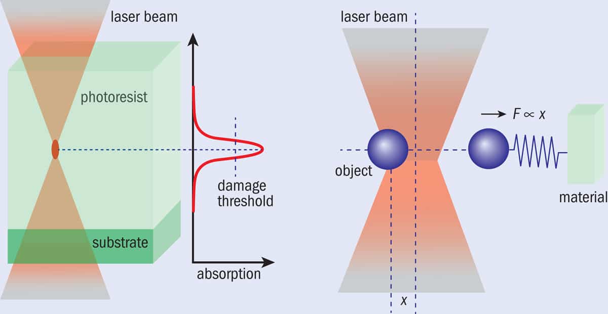 Printing functional nanoscale devices calls for sophisticated optical techniques. Two-photon polymerization (left) allows a finer resolution than is possible with more common single-photon absorption methods. By using photons with half the energy required to drive a polymerization reaction, the two photons need to be absorbed within a very short timescale. Because this process is proportional to the square of the intensity of photons incident on the target, only in the most focused regions of the incident light – when using a high numerical aperture and a femtosecond-pulsed laser – will two-photon absorption occur, therefore resulting in high resolution and feature sizes of the order of 100 nm. By coupling this set-up with an optical-tweezer arrangement, whereby very small forces can be exerted on an object through the focusing of a laser beam (right), larger micron-sized objects can be drawn into the vat of material and encased within a matrix or attached to a surface. This offers the potential for functionalizing a surface or a material by combining it with particles prepared separately and then brought together.