Infrared vision could help the blind to see

Researchers in the US have developed a prototype retinal implant that they hope will help to restore sight to patients blinded by the loss of light-detection cells in their eyes. Although it is not the first such device – other scientists have already conducted human trials on retinal implants – this latest device is the one of the first to work without an external power source. The researchers believe this should make it easier to miniaturize the circuitry involved, allowing higher-resolution vision.

One of the most intriguing areas of research into medical prosthetics – and, in some cases, treatment – is the development of retinal implants. These aim to restore some degree of sight to patients blinded by conditions such as age-related macular degeneration or retinitis pigmentosa. In these conditions, the photoreceptors in the eye decay while the neurons that carry the signal to the brain remain intact. It is possible, therefore, to restore some degree of sight by implanting a light sensor on the retina and using the electric current to stimulate the neurons.

Wireless solution needed

Early designs for retinal implants usually required an external power source to be wired into every pixel of the implant. This limits the minimum pixel size and thus the resolution that can be obtained. So Keith Mathieson, James Loudin, Daniel Palanker and colleagues at Stanford University have developed an alternative that is powered by the incoming light itself. This has obvious appeal because, as Richard Taylor, who works on retinal implants but was not involved in the new research explains, “no-one wants a wire in their eyeball!”. The concept has proved a great challenge, however, because there simply isn’t enough energy in visible light to produce the electricity needed to stimulate neurons.

The Stanford team’s solution involves the patient wearing special goggles that receive incoming visible light and process the image before transmitting information about it into the eye as a series of infrared laser pulses. Powering the goggles, which joint lead author James Loudin describes as “the exact opposite of night-vision goggles, which convert infrared radiation into visible light”, is much simpler than powering retinal implants.

The amplified infrared pulses pass through the eye to a sub-retinal implant comprising an array of infrared photodiodes. These photodiodes convert the infrared radiation into electrical signals, which stimulate the surviving neurons. Although the neurons will only occasionally receive a brief pulse of electricity from the photodiodes, Loudin does not anticipate that this will cause a problem. “The human eye only has a bandwidth of a few tens of hertz anyhow,” he says, “which explains why movies look continuous even though they are actually delivered at 25 frames per second.”

Test-tube study

The team’s current paper describes a test-tube study using the set-up to stimulate electrical responses from both healthy and degenerate rat retinas using infrared light. The researchers are now studying their implant in live rats. Loudin is pleased with the results, which are currently awaiting publication. Ultimately, the team would like to test the technology in humans, which remains the ultimate goal, but on this point Loudin is cautious. “At present this remains an academic study with no commercial entity associated with it,” he says, “although we’re open to receiving such offers.”

Psychologist, physicist and artist Richard Taylor of the University of Oregon in Eugene believes that the research makes a valuable contribution to the growing field of work in treating this type of blindness. “From my view,” he says, “the best long-term solution is to develop a chip that replicates the function of the diseased photoreceptors – the approach taken here.” He explains that commercial companies on both sides of the Atlantic have made considerable headway with this approach, but they have been hamstrung by the need to power the implant.

“In the current work, the researchers make use of near-infrared physics to deliver a very appealing solution. Perhaps most crucially, they show that this design can work using radiation intensities substantially below the safety limits for the visual system,” he concludes. “This is a very impressive demonstration.”

The research is published in Nature Photonics.

How significant would the discovery of the Higgs boson be?

By James Dacey

hands smll.jpg

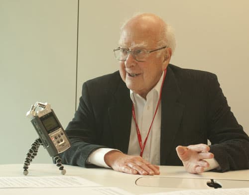
His eponymous particle may be famously elusive, but Peter Higgs has been seemingly omnipresent in Bristol over the past couple of days. He has spent today at Physics World headquarters, having appeared last night at the Bristol Festival of Ideas, and he has just shot off to the University of Bristol to meet with academics and give a special colloquium. Last night he also managed to squeeze in an appearance on the local news programme BBC Points West, which documented Higgs returning to Cotham School, where he was a pupil for five years. You can read full details of Higgs’ Bristol trip in this blog entry by Physics World editor Matin Durrani, who spent time with Higgs today to record an interview that will be appearing on physicworld.com.

In Higgs’ talk last night, he was joined on stage by the science editor of the Observer, Robin McKie, and naturally the questions turned to the particle that now bears his name. When asked about how he came up with his boson, Higgs lived up to his famous modesty, explaining how the idea had emerged without grand designs from his work on a problem relating to superconductivity. He seemed slightly embarrassed that the particle has been named after him when there were several other theorists working on the same issues.

Higgs was also humble when questioned about how he felt about the vast investments that have been made in constructing particle accelerators to hunt (in part) for the fruit of his work. When asked by a member of the audience whether he would celebrate the discovery of his boson, Higgs replied in his typically understated manner that he has a bottle of champagne left over from Christmas, but he that he hadn’t yet “put it in the fridge”.

In this week’s Facebook poll we want to know how you feel about the hunt for the Higgs boson.

How significant would the discovery of the Higgs boson be?

It would answer the biggest outstanding question in physics
It would answer the most important question in particle physics
There are other more important questions in particle physics

Let us know by visiting our Facebook page. And please feel free to explain your response by posting a comment on the Facebook poll.

In last week’s poll we asked “What is your primary source of online physics news?”. 78% of respondents said they get the majority of their updates from specialist news sites. 9% said they rely on general news sites. 6% use social media, another 6% rely on blogs, and just 1% get their news via Internet radio and podcasts.

Thank you for your participation and we look forward to hearing from you in this week’s poll.

Higgs spotted in Bristol

Peter Higgs

(Courtesy: Dirk Dahmer)


By Matin Durrani

It’s been a hectic few days for 82-year-old Peter Higgs.

The retired Edinburgh University particle theorist, after whom the famous boson is named, has been in Bristol for the last two days undertaking a series of public engagements.

First up was a visit yesterday to Cotham School, where Higgs was a pupil for five years during the Second World War when his father – a BBC engineer – was posted to the city. Higgs is in fact not the only great physicist the school has produced – the other stellar pupil was Paul Dirac, whose name the young Higgs used to see displayed prominently on the school’s honours boards. Higgs, who was back at the school for the first time since the war, signed autographs as he opened a new science block, appropriately named The Dirac–Higgs Science Centre, accompanied by the media.

In the evening, the self-effacing Higgs then took part in an event at St George’s Bristol that was part of the city’s Festival of Ideas. In front of an audience of several hundred people, he was joined on stage by Graham Farmelo, author of the award-winning Dirac biography The Strangest Man, who outlined Dirac’s achievements and his links with Bristol. Higgs then took part in a conversation with Observer science editor Robin McKie, who asked him, among other things, how he would celebrate if the Higgs boson is found. To much amusement, Higgs replied that he had “a leftover bottle of champagne from Christmas” but that he hadn’t yet “put it in the fridge”.

Today, Higgs paid a visit to IOP Publishing, where I interviewed him for Physics World. Inspired by questions posted by readers on our Facebook page and sent to us via Twitter, I quizzed Higgs about his early work on symmetry breaking, his thoughts about the search for the Higgs at CERN and his wider views on physics. We’ll be posting the interview online in the next month or two, so stay tuned for that.

Higgs still remains embarrassed at having a particle named after him, feeling that it places too much of the credit on him at the expense of other theorists. But during our interview, even he on occasion dropped the “so-called” from the “so-called Higgs boson”, the “so-called Higgs field” and the “so-called Higgs mechanism”. It just gets tiring after a while, I suppose.

As I write, the indefatigable Higgs is off to give a colloquium in the main lecture theatre at the physics department at the University of Bristol, entitled “My life as a boson”. Over lunch I asked Higgs if that wouldn’t be the perfect title for his autobiography. Self-effacing as ever, Higgs replied that, when it came to writing books, he was simply “too lazy”. So if you want to hear more about his life, you’ll have to wait for the Physics World interview.

Levitating drops controlled by fridge magnets

A team of scientists in France has shown that it is possible to control a paramagnetic liquid drop using a magnetic field at room temperature. Using a drop of liquid oxygen, they show that the drop’s trajectory can be controlled using a magnet. The work could help with the development of highly hydrophobic materials and also with the study of very low-friction mechanical systems.

Vapour cushions

The team’s drops are an example of Leidenfrost drops. The Leidenfrost effect is seen when a liquid comes in contact with a surface that is at a significantly higher temperature than the liquid’s boiling point. This produces an insulating layer of vapour that keeps the drop from evaporating rapidly. As there is no contact between the drop and the surface, the friction of the system is reduced dramatically, which makes the drops highly mobile and difficult to control. Indeed, such systems could be considered as the ultimate hydrophobic systems – wherein the liquid is complexly detached from the solid surface.

While this “liquid levitation” was discovered in the 1960s and is used in the some industries, the fundamental physics of the phenomenon have not been studied. In this latest research, David Quéré and colleagues at Ecole Polytechnique in Palaiseau have looked into the forces that drive liquid-oxygen drops, which boil at –183 °C. They have created methods to control the motion of the drops and have also studied how the drops interact with a magnetic field. The research follows on from previous studies by the team and others that looked at developing textured surfaces that make the Leidenfrost drops self-propel with a very high velocity in all directions.

Levitating drops

A highlight of this latest study is the discovery that the drops can be controlled using a simple fridge magnet. In the experiment, the researchers produce the liquid-oxygen drops by pouring a litre of liquid nitrogen into a metal container. “The oxygen drops form as condensation on the outside of the container,” explains Quéré. “In addition to being a really simple process, it’s interesting too, as for once you actually ‘see’ oxygen,” he says. After producing their drops, the researchers placed them on glass plates, with the magnet below.

They found that the magnet had a strong effect on the motion of the drops. Quéré describes the interaction as “rich”. “The system could almost describe celestial mechanics. The magnet acts as the Sun and determines the trajectory of the drop that acts as a planet. But the interactions are even better as we don’t just see elliptical orbits. We see the drops following complex trajectories, forming loops even before breaking away,” he explains.

Sculpting drops

Another interesting aspect of the interaction occurs when a drop passes directly above the magnet. The researchers found that the drop slows down and is nearly trapped by the field. When it breaks away, the shape of the drop is deformed. Quéré points out that this is interesting in a much wider physical context, because the deformation is caused by a transfer of kinetic energy. “Just like when a raindrop hits the ground, it loses most of its energy as it gets deformed upon impact. This transfer of energy is interesting and depends on many parameters,” says Quéré. He told physicsworld.com that the new approach offers a way to study such deformations in a system with negligible friction.

The researchers can change the amplitude of these deformations by changing the strength of the trap – simply by moving the magnet closer to or away from the plate. Quéré says that the team looked into more ways to use a magnet to “sculpt” a drop – for example using an annular (ring-shaped) magnet to get a torus-shaped drop. The researchers then remove the magnet and study the doughnut-shaped drop until it closes again.

Gravitational slingshot

The team also managed to accelerate the drops out of the trap using a method that is normally used to modify the speed of a spacecraft by using the gravity of a planet or a moon to propel it – the so-called gravity-assist technique or the “gravitational slingshot”.

“We think that this system is a great way to study complex celestial mechanics, where the gravitational influence is replaced by the magnetic influence,” says Quéré. “It’s like having a little piece of sky!” Quéré also says that the work will help in further developing non-wetting techniques in micro-engineering, where water and oil travel down the same channel but must not touch.

The paper is to be published in Physical Review E.

Reality bites

The evolutionary biologist and prominent atheist Richard Dawkins has often lamented the fact that physicists are much less antagonistic to religion than biologists are. He attributes this split to biologists’ greater familiarity with Charles Darwin, who showed clearly that humans could evolve by natural selection without any need to invoke divine intervention.

I, on the other hand, think that we physicists are friendlier to religion simply because, in the final analysis, we are closer to God. Before anyone jumps all over me, let me clarify that I am using the word “God” purely metaphorically. In other words, in my language, as in the language of most physicists, “closer to God” simply means “more fundamental”. Physics is the most fundamental of sciences because chemistry is really just an application of quantum physics, and biology is completely underpinned by organic chemistry. This description must be taken with a grain of salt, since no-one really knows how to formally derive chemistry and biology from quantum physics. However, most physicists believe that all natural sciences are fully compatible, and that if you look closely enough at any of them, you will find physics principles at work.

Given my strong physics bias, I was particularly delighted when Physics World asked me to review The Atheist’s Guide to Reality. Author Alex Rosenberg is a philosopher at Duke University in the US, and he subscribes to exactly the reductionist logic I summarized above. As he puts it, “physical facts fix all facts”, and there are no phenomena in this universe (including not just chemistry and biology, but psychology and sociology as well) that cannot be explained from the laws of physics. His book is basically an exposition of the philosophy that, he argues, naturally follows from this world-view. For lack of a better word, he calls this world-view “scientism” and the resulting philosophy “a nice form of” nihilism.

As the title of his book suggests, Rosenberg believes that if the laws of physics fix all the facts, this leaves no room for a god. His answers to other tough questions are similarly pithy. Q: Is there a soul? A: You’ve got to be kidding! Q: What is the nature of reality? A: What physics says it is (hence “scientism”). Q: What is the purpose of the universe? A: There is none (hence “nihilism”). Similarly, Rosenberg states that there is no meaning to life; you and I are here because of dumb luck; and the only lesson we can learn from history is that there are no lessons from history, because the random element in the universe prevents history from ever repeating itself.

Rosenberg’s book is well written and full of witty one-liners that will make you laugh. His advice for countering depression caused by nihilism, for example, is to pop a couple of Prozacs. He also makes a well-presented and plausible argument for why we find science counterintuitive – and why evolution has made us prefer storytelling to doing long and hard mathematical calculations. The gist of the argument is that survival requires us to make quick and dirty evaluations of other people and situations. Stories are a much better storage medium than formal mathematics for the rules of thumb we use to make decisions. This is why we prefer reading fiction to non-fiction and believe in myths despite a complete lack of scientific evidence.

Such arguments go a long way towards explaining why there is discord between our intuitive picture of reality (which includes supernatural events, gods, the simple division into “good and bad” and so on) and what science tells us is really at the core (i.e. nothing). However, this has all been seen before in the recent popular literature such as Geoffrey F Miller’s excellent The Mating Mind: How Sexual Choice Shaped the Evolution of Human Nature (published in April 2000 by Doubleday in the US, Heinemann in the UK). I have not really learned anything new from Rosenberg here, though he does tell it in an engaging and original way.

I am an atheist who likes to think that physics underlies all other sciences. But somehow, to my great surprise, the deeper I went into the book, the more I disagreed with Rosenberg’s conclusions. What bothers me most is the strength of conviction with which Rosenberg pursues many of his key arguments. For instance, he claims that natural selection follows from physics, and “The second law [of thermodynamics] makes evolution inevitable.” Inevitable? Really? If true, this is certainly news to physicists and biologists. In fact, many scientists maintain that, contrary to the purely reductionist picture I presented earlier, biology can never be derived from physics, not even in principle, even though both chemistry and biology are fully consistent with quantum physics. Even worse, physicists are still arguing about how to derive the laws of thermodynamics from microscopic dynamics. A subtle and intriguing point that Rosenberg misses is that the validity of thermodynamics is independent of the details of the microscopic laws. In other words, not only might physical facts not fix all facts, but some physical facts are not even uniquely fixed by other physical facts.

Rosenberg also claims that the laws of physics themselves can be explained (without a god) by taking a “multiverse” perspective. This argument dates back to the ancient Greeks, and especially to pre-Socratic philosophers such as Democritus, who in effect argued that all possible universes exist with all possible laws and we are merely living in one such universe. This is okay as far as it goes, but then Rosenberg claims that our best current theory suggests that our universe is one in a multiverse. Oh yeah? Our best current theory is the Standard Model of particle physics, and it suggests no such thing. And besides, what possible evidence can we have for other universes with other laws of physics? It is easy to see why the existence of all possible universes appeals to scientifically minded atheists, since it could solve the “Goldilocks” problem (our universe appears to be fine-tuned to our existence) without invoking a deity. However, this is not in itself a strong enough reason to promote it.

One could argue that the above flaws are only tangential to Rosenberg’s main point and ought to be forgiven in a popular-philosophical book. Fine. I, too, frequently cut corners when writing for popular audiences. But I think even Rosenberg’s broader philosophy misses the point of science, which is to remain in a state of suspended judgment: you make a conjecture and you wait to see what happens in experiments. It is precisely those who are unable to suspend judgment, who cannot wait or are scared to live without a definitive answer to every question, who need some kind of religion to give them comfort. In some sense this makes Rosenberg himself a religious person, even though he strongly embraces atheism. This might seem like a contradiction, but it is not: being “religious” in this sense does not necessitate believing in a god – a point well illustrated by the existence of communism.

There is something magical about science that is completely absent from Rosenberg’s cold and clinical philosophy. Feynman called physics “the most exciting adventure that human imagination has ever begun”. But not only is it exciting, it also requires a great deal of imaginative work. Its whole point is to enrich our world-view. In the words of the US naturalist John Burroughs, “the final value of physical sciences is its capability to foster in us noble ideals, and to lead us to new and larger views of moral and spiritual truths”. Regrettably, you will not find any of that in Rosenberg’s book. If you wish to read about the uplifting feeling that science really fosters, you would be much better off with Carl Sagan’s The Demon-Haunted World: Science as a Candle in the Dark.

  • Buy now with 30% discount for physicsworld.com readers (enter code WN196 at the checkout)

Graphene comes of age

Since its discovery in 2004, graphene has rapidly attracted the attention of academic and commercial institutions, which are looking to develop new technologies from the material. These include speedy electronics and communications devices, and a new generation of highly efficient solar cells.

The fundamental science of graphene and its potential applications are subjects of great interest to Patrick Soukiassian, a scientist who has spent several decades researching nanotechnologies and semiconductor materials. In this video interview, Soukiassian, of the University of Paris-Sud/Orsay and CEA-Saclay, explains that the vast potential of graphene has now been recognized by the European Union, which is starting to invest in several initiatives to support the development of these technologies.

In a separate video recorded last year, I visited the University of Manchester in the UK to learn how graphene can be made using nothing more than a sheet of graphite and some sticky tape.

But in order to develop applications, scientists are now seeking ways to produce high-quality graphene in large quantities. Soukiassian identifies one promising approach that involves growing sheets of graphene crystals on an underlying substrate of silicon carbide. The fact that this method is silicon-based means that it can borrow techniques that have already been refined over many years in the computing and electronics industries.

This field of research, known as epitaxial graphene, is the subject of a recent special issue of Journal of Physics D: Applied Physics, of which Soukiassian is an associate editor. The collection of papers, guest edited by Walt A de Heer of Georgia Institute of Technology, US, and Claire Berger of Georgia Institute of Technology and CNRS-Institut Néel, France, addresses the science and technology behind epitaxial graphene, both its production and its physical properties. The issue is free to read until the end of June 2012.

  • Graphene compilation Discover the must-read research on this expanding topic across eight leading physics journals from IOP Publishing

Photon-polarization qubits stored in atomic combs

Three independent teams of physicists have created the first solid-state quantum memories that store the polarization states of photons. While the three systems each use different materials, they are all based on the concept of an “atomic comb” – whereby a photon is stored in a collective excitation of the atoms within the solid.

Photons have proved to be a good choice for transmitting quantum bits (qubits) of information because they can travel for long distances without interacting with their surroundings. Their other advantage is that quantum information can be stored in a photon’s polarization state, with “1” represented by horizontal polarization and “0” by vertical, for example.

Unfortunately, it is very hard to make a quantum memory that can store photon qubits, which has been bad news for anyone wishing to make a quantum computer or build “quantum repeaters” that allow quantum information to be transmitted over long distances. Physicists have been able to create solid-state memories that can store and re-emit qubits based on the temporal properties of light – “1” for the presence of a photon and “0” for its absence, for example – but not the photon’s polarization itself.

One problem is that many solids tend to cause bifringence – a refractive effect that sends light of different polarizations along different paths. The other snag is that the degree to which many solid materials absorb light depends on the polarization of the light. The bottom line is that it is very difficult to make a device that stores a qubit with an arbitrary polarization.

Triple pronged

To get round this problem, the three groups took surprisingly simple approaches. Two teams – one led by Chuan-Feng Li at the University of Science and Technology of China in Hefei and the other by Mikael Afzelius at the University of Geneva – made their memories from two crystals of the same material that are rotated by 90 degrees to each other.

Meanwhile at the Institute of Photonic Sciences in Barcelona, Spain, Hugues de Riedmatten and co-workers used one crystal but split the incoming light into two separate beams, one of which has its polarization rotated by 90 degrees. The two beams are then sent through the crystal, and the emerging rotated beam is then rotated back to its original polarization before the two beams are recombined.

In all three cases, the basic idea is the same – by rotating one crystal or beam polarization by 90 degrees, the problems of bifringence and directional absorption are effectively eliminated. Quantum information is stored in each case in an “atomic frequency comb” (AFC) – a phenomenon first identified in 2009 at the University of Geneva by a team that included Afzelius and De Riedmatten. An AFC is a collective excitation of atoms in a crystal that includes a large number of frequency modes that are equally spaced in energy, like the teeth on a comb.

Drifting out of phase

The storage process begins when the photon is absorbed and excites the AFC modes. The modes then evolve in time such that they drift out of phase with each other. While this occurs, the AFC is unable to re-emit the photon. However, after a fixed amount of time – typically tens or hundreds of nanoseconds depending on the material – the comb modes are back in phase with each other and the photon is re-emitted with the same polarization as the absorbed photon.

The Geneva and Barcelona groups used yttrium-orthosilicate crystals that were doped with neodymium and praseodymium, respectively, while the Hefei team used yttrium-orthovanadate crystals doped with neodymium.

All three teams are currently trying to improve their devices. Li told physicsworld.com that the Hefei team is working on how to store multi-photon polarization entanglement in several different quantum memories. Afzelius’ team is investigating how the storage time can be extended to millisecond or even second timescales by using different materials, which is important given that storage times of seconds are needed for practical quantum repeaters. Meanwhile in Barcelona, De Riedmatten and colleagues are looking at how the AFC excitation can be transferred to a spin excitation in the solid – a process that they believe could be used to boost the storage time to a few seconds.

The research is described in three papers in Physical Review Letters.

Physicist convicted of terrorism leaves prison

Adlène Hicheur, the particle physicist convicted of terrorist charges, has been released less than two weeks into his four-year prison sentence, according to his former supervisor. Jean-Pierre Lees, a researcher at the Particle Physics Laboratory in France, told physicsworld.com that Hicheur was released from a French jail on the night of Tuesday 15 May, just one day after the deadline for him to appeal his guilty verdict had elapsed. According to Lees, Hicheur had considered appealing the verdict but in the end had decided against it because it would have required him to remain in prison for an additional eight months.

Hicheur, a 36-year-old French-Algerian, was arrested by French police on 8 October 2009 on suspicion of having links with the organization Al-Qaida au Maghreb islamique (AQMI). Prior to his arrest, Hicheur was working as a postdoc at the Swiss Federal Institute of Technology in Lausanne and spent time at the Large Hadron Collider at CERN. Hicheur remained in custody without charge for almost two and a half years – the maximum time permissible under French anti-terrorism laws

In November 2010 Lees sent a letter to the French Physical Society expressing concerns about the continued imprisonment of Hicheur without charge that was signed by 19 physicists including the Nobel laureate Jack Steinberger. Hicheur also received support from an “international defence committee”, consisting of about 100 scientists, which wrote to the French authorities, including the then French president Nicolas Sarkozy.

Focus on e-mail exchange

Hicheur’s first hearing took place on 16 February this year and the case came to a close on 4 May as Hicheur was found guilty of “participation in a conspiracy to prepare an act of terrorism”. The trial’s official summary document is centred on an exchange of e-mails between Hicheur and a contact with an alleged affiliation to AQMI, which took place between 2008 and 2009 while Hicheur was based in French territory. The trial document states that Hicheur appears to have given “financial support” to his contact in AQMI by offering to transfer between €5000–8000 to them. The summary also states that a folder was discovered on Hicheur’s personal computer with the name AQMI.COMS.

But Hicheur’s supporters, including Lees, feel that the sentence was a miscarriage of justice. “No proof that he sent money to this people [sic] has been shown, while all his bank accounts have been carefully scrutinized,” says Lees. He also questions the decision of the court not to summon the suspected AQMI terrorist to ascertain the true identity of this person and to establish whether Hicheur was fully aware with whom he was liaising.

“The instruction judge had no choice but to demonstrate by any means the involvement in a terrorist project, and so had to condemn Adlène to justify the two years and eight months he had already spent in jail,” says Lees. “The justice, like the medicine, rarely recognize its errors.”

‘A Kafkian situation’

Francesco Spano, a particle physicist at Royal Holloway, University of London, is also highly critical of the French justice system in its handling of the Hicheur case. “I am outraged by the fact that a person can be kept captive for about two and a half years without being judged, in a Kafkian situation,” he said. “During the trail it was hard for me to find the evidence for the specific material facts that would support the accusation”. Spano, who is one of 342 members of the Adlène Hicheur International Support Committee (CISAH), says that he would like this group to now focus on two goals: to help Hicheur to rebuild his life, and to try to understand the implications of this trial to society.

Another group that helped to raise the profile of the Hicheur case is ConCERNed for Humanity, which was seeking the support of the CERN management and the lab’s international community of users. One of the group’s members Michael Dittmar, a researcher based at ETH Zurich and CERN said that he will continue to support Hicheur and echoed the criticism of the French anti-terror laws. “Perhaps one might have some very remote hopes that the new French government can also lead to a more open position of the management,” he said.

A cracking approach to nanotechnology

For most manufacturers, cracks are usually something to be avoided – and the semiconductor industry is no exception. But now engineers in South Korea have shown how initiating and then controlling the spread of nanometre-sized cracks can be used to create pre-designed patterns in a silicon wafer. They say that their approach offers a potentially faster and cheaper alternative to conventional lithography for the fabrication of integrated circuits.

Cracks can form when two materials with mismatching crystalline structures are placed on top of one another. Stress builds up at the interface between the materials, deforming the crystal structures and creating a crack that spreads throughout both materials if the deformity builds up enough potential energy to break atomic or molecular bonds. This can happen when a thin layer of silicon nitride is deposited on a silicon substrate, with cracks spreading uncontrollably through one or both of the layers.

Koo Hyun Nam of the Ewha Womans University in Seoul and colleagues have controlled the formation of such cracks to create elaborate patterns within a silicon substrate. To do this they etched tiny structures at particular positions and with specific orientations within 0.5 mm-thick silicon wafers. The idea was that these “micro-notches” would concentrate the stress resulting from the deposition of a thin film of silicon nitride on the substrate. They also carved out step-like structures within the substrate to halt the spread of cracks or to isolate certain regions of the wafer from cracks.

Wavy cracks

Using chemical vapour deposition to lay down the silicon nitride, Nam and co-workers found that the cracks formed and propagated spontaneously. They were able to make the cracks either straight or wavy by changing the orientation of the crystal planes in the wafers as well as adjusting other parameters such as the temperature and pressure of the vapour. By laying down a film of silicon dioxide between the substrate and the silicon nitride they were able to generate a third shape – “stitch-like” cracks, which are straight cracks with short, parallel, angled branches.

The width of the cracks varied between about 10–120 nm, with the wavelike variety generally wider than the straight cracks. In addition, the researchers found that they could change the direction of a crack, causing it to “refract” much like a light wave passing into and then out of a block of glass, by separating only a part of the wafer and the silicon nitride with the silicon-dioxide film. Where there was no silicon dioxide, the crack penetrated more deeply into the silicon substrate and aligned itself more closely with the substrate’s atomic planes, whereas this alignment was weaker where there was silicon dioxide, causing the crack to change direction in this region.

Writing in Nature, Nam’s team says that this method of controlled cracking could offer a faster and cheaper alternative to conventional lithography for microchip fabrication. In an accompanying article, Antonio Pons of the Polytechnic University of Catalonia in Barcelona, Spain, agrees. He says that lithography, which allows patterns to be etched in silicon using a mask created via beams of light, electrons or ions, is often complex, expensive and time-consuming.

Hours, not weeks

Pons told physicsworld.com that the advantage of the new approach is that the time needed to form the pattern “is simply the time taken for the crack to propagate”, estimating that it should take only a few hours altogether to prepare the substrate, deposit the film and create the pattern, compared with the “days or weeks” needed using standard lithography. He admits, however, that he does not know how long it would take to make the micro-notches and other features. He also says it remains unclear how closely the cracks can be positioned to one another, something, he points out, “that is crucial when making small structures”.

But Pons believes that the new technique should also find applications beyond the semiconductor industry. One possibility, he says, is making microfluidic devices. These are networks of tiny channels within which fluids, containing molecules such as DNA, can be manipulated for study. He also wonders whether it might prove useful at larger scales, perhaps allowing buildings in earthquake zones to fracture more safely. “The answer to that is not necessarily yes,” he says. “Scale is very important, and we would be going from atomic-level interactions to the size of a house. But maybe this work will inspire people in other fields.”

Zhenan Bao, a chemist at Stanford University in the US, says that the strength of the latest work is in showing the formation of controlled cracking, pointing out that other groups have previously used cracks to create nanoscale patterns, but that they were not able to carefully control where the cracks formed. Bao cautions, however, that such controlled cracking would only be possible with certain combinations of materials, which may mean the technique has more limited appeal than standard lithography. “It would be nice to see a demonstration of this method for device application,” she adds.

Quantum dots give graphene photodetector a boost

Researchers in Spain have fabricated a new, highly sensitive photodetector from graphene and semiconducting quantum dots. The device is a billion times more sensitive to light than previous graphene-based photodetectors and might be ideal for a variety of applications, including light sensors and solar cells, infrared cameras for night vision and in biomedical imaging.

“In our work, we managed to successfully combine graphene with semiconducting nanocrystals to create complete new functionalities in terms of light sensing and light conversion to electricity,” says Gerasimos Konstantatos, who was co-leader of the team at the Institute of Photonic Sciences (ICFO) in Barcelona. “In particular, we are looking at placing our photodetectors on ultrathin and flexible substrates or integrating the devices into existing computer chips and cameras,” adds co-leader Frank Koppens.

Graphene is a sheet of carbon atoms arranged in a honeycomb-like lattice just one atom thick. The material could find use in a number of technological applications and in the future could even replace silicon as the electronic industry’s material of choice, thanks to its unique properties. These include extremely high electrical conductivity, which comes about because electrons whizz through graphene at extremely high speeds, behaving like “Dirac” particles with no rest mass.

Ideal internal quantum efficiency

Graphene also shows great promise for photonics applications because it has an ideal “internal quantum efficiency” – almost every photon absorbed by the material generates an electron–hole pair that could, in principle, be converted into electric current. Thanks to its “Dirac” electrons, it can also absorb light of any colour.

However, all is not perfect because graphene’s “external quantum efficiency” is low – it absorbs less than 3% of the light falling on it. Another problem is that useful electrical current can only be extracted from graphene-based devices that have electrical contacts with an optimized “asymmetry” – something that has proven difficult to achieve.

Koppens, Konstantatos and colleagues began with a piece of high-quality graphite from which they obtained graphene flakes using the now-famous “Scotch tape” technique. This involves placing the graphite sample on a piece of sticky tape then folding and unfolding the tape a few times until some grey transparent pieces of material can be seen among the original black and shiny fragments of graphite. Next, the researchers press the tape with the transparent graphite onto a substrate and then remove the tape.

“We can see many pieces of graphite with varying thicknesses on the substrate, and look for the ones with the lowest contrast – these are graphene,” explains Koppens. “It is remarkable that we can see a one-atom-thick layer of material with the naked eye, but that is thanks to graphene’s unique interaction with light.”

Hybridizing with quantum dots

The teams then used nanoscale lithography to contact a sample of graphene to two gold electrodes for subsequent electrical measurements. The electrodes are positioned with sub-micron precision in a process whereby gold is evaporated onto a resist mask especially drawn for the flakes with an electron-microscope gun. The next step is to hybridize the graphene with colloidal semiconducting quantum dots that photosensitize the carbon material.

“We chose quantum dots because of their unique optoelectronic properties,” says Konstantatos. The materials can be tuned to absorb a wide range of light wavelengths simply by changing the size of the nanocrystals. They also absorb light very strongly. Moreover, the dots can be processed in solution and can thus be sprayed, spin cast or ink-jet-printed onto any substrate, including graphene, at low temperatures and in air – non-negligible advantages that could bring down costs and simplify fabrication.

The researchers used lead-sulphide quantum dots because the band gap in these semiconductors can be tuned in the technologically important short-wavelength infrared (SWIR) and near-infrared (NIR) ranges.

Tailored connections

“A critical part of our experiment involves ligand exchange to cross-link the quantum dots with short (around 0.2 nm) molecules and attach these to the graphene,” explains Konstantatos. “This step was needed to passivate the surface states in the quantum dots and so allow for efficient charge-carrier transfer to graphene and suppress unwanted recombination of electrons and holes – which would have lowered the amount of current eventually produced by the finished photodetector.” The challenge was to tailor the electrical connections between the semiconducting nanocrystals and graphene while maintaining the high quality and exceptional electrical conductivity of this material, he adds.

After depositing a thin film of the quantum dots on the graphene, the ICFO researchers characterized their device by exposing it to light while probing its resistance at the same time. The photodetector responded to tiny amounts of light (almost complete darkness), as seen by the large change in its resistance.

Since the device was designed in a transistor arrangement, it was possible to change the carrier density in the graphene by varying the voltage on the gate electrode. “From these measurements, we could very precisely quantify the internal quantum efficiency of the device as being greater than 25% because the quantum dots absorb light so well and because charge transfer between the two materials is so effective,” says Koppens. “We found that we could also optimize this performance with the voltage on the gate or even switch off the response. This ‘switchability’ might come in useful for pixelated imaging techniques.”

Bendy solar cells

Many of today’s photonic devices rely on ultra-efficient conversion of light to electricity, Konstantatos adds. “Our detector could be used in digital cameras, for night vision and in biomedical imaging, as well as in sensing applications. Its flexibility also means that it might be ideal for bendy solar cells that could be placed on objects of any shape – an avenue that we are currently exploring.”

The team now plans to scale up the detector to large-scale imaging arrays. “We expect that most cars will be equipped with night-vision systems in the near future and our arrays could form the basis of these,” says Koppens. The researchers also aim to improve their device even further so that it can detect single photons.

The current work is detailed in Nature Nanotechnology.

Copyright © 2025 by IOP Publishing Ltd and individual contributors