‘Pushy’ electrons move atoms

Researchers in the US have gained important new insights into how electrons travel through nanoscale metal wires. They discovered that the force with which electrons push atoms around in these structures is much stronger than previously thought – which could help improve next-generation nanoelectronic components.

As electronic devices become ever smaller, researchers need to better understand how electrical currents affect the atomic structure of tiny circuits. In particular, the electromigration of atoms in a nanowire could alter its electronic properties – or even cause it to fail. On a positive note, this movement of atoms could be used to assemble tin structures.

Ellen Williams and colleagues at the University of Maryland began their study by creating a range of different nanoscale structures, such as islands and “steps” (that contain between 100 and 100,000 atoms), on top of very thin silver wires measuring 2 to 50 nm across. The researchers then used a scanning tunnelling microscope to observe how the structures moved or changed shape when a current was sent through the wire. “It was amazing – when we changed the direction of the current, we found that we could the move the structures back and forth,” Williams told physicsworld.com.

Twenty times stronger

The Maryland team says that the force with which charge carriers (in this case electrons) push atoms around in such nanostructures is much stronger – by up to 20 times – than previously thought. According to the researchers, this strong “electromigration force” could be used to intentionally move atoms around in nanoelectronic components – something that might help in self-assembling nanowires, for example, to create devices that can be cycled through different structures under an alternating current. It may even be used to move nanomachines in the future.

And that’s not all: the team also found that the electromigration force could be greatly decreased by an adding an electron-withdrawing structure (or defect), such as C60, along monatomic step edges.

The different ways that electrons can move through a nanowire can be described by how easily electrons travel, or are transmitted, through the structure, explains Williams. Most atomic structures allow electrons to travel through easily but defects slow down electron movement. This results in a local “resistivity dipole”, which means that the defect sites have a local resistance and local electrical field very different from that in the rest of the material. “The key point is that the special atomic structures of defects cause weak transmission of electrons (or strong scattering),” she said.

Graphene is next

Williams’ team is now studying similar effects in nanoscale structures on top of graphene (sheets of carbon just one atom thick) as well. “Our group has been creating defect structures of graphene and deposing small amounts of scattering atoms onto the carbon material,” revealed Williams. “Using our powerful microscope techniques, we expect to see comparable effects of atomic motion and local resistances when graphene is carrying current.”

The results of this work might eventually lead to new ways of exploiting graphene’s unique electronic properties, she says.

The work was reported in Science 328 737.

All together now…

chair.jpg

With a little help from their friends: some of the DØ collaboration

By Hamish Johnston

Many years ago I wanted to be an experimental particle physicist (didn’t you?).

But then I cast my eyes over a few papers and realized that my name would be buried between D Johnston and A Jonckheere in a two-page list of authors (if I was lucky enough to join the DØ collaboration above).

I can’t say that was the only reason that I switched to condensed matter physics – I found it more interesting, for example – but the idea of being a small cog in a huge machine wasn’t that appealing.

Since then I’ve often wondered how hundreds (indeed, thousands) of particle physicists get together to write one paper.

If you are curious, Tommaso Dorigo has a blow-by-blow account on his blog.

Among other things, it involves committees referred to as “godparents” and arguments over British versus American spellings – although I would have thought the journal would have the last word on the latter.

Dorigo writes, “Now, if you think that the above baroque, surreal, ridiculous procedure is crazy, you might be right”.

However, he also points out that the process is “extremely democratic”, which he says is one of its “striking positive qualities”.

But is democracy the best way of doing science?

Cast your ballot now!

It’s high-NOON for five photons

Physicists in Israel are the first to entangle five photons in a NOON state – the superposition of two extreme quantum states. Unlike previous schemes for creating such states, the researchers claim that their new technique can entangle an arbitrarily large number of photons – so called “high-NOON states”. This could be good news for those developing quantum metrology techniques because high-NOON states could be used to improve the precision of a range of different measurements.

In Schrödinger’s famous thought experiment, all of the molecules in a cat are in a superposition of two extreme states – living and dead – and an observer cannot tell which until a measurement puts the cat into one of the two states. Such extreme “Schrödinger’s cat states” can, however, also be made in the lab. Ideally, this could involve splitting a pulse of N photons and sending all N photons down one of two orthogonal paths. The photons would be in a superposition of both paths – called a NOON state after how it is written mathematically.

NOON states are of particular interest in quantum metrology because if the light is recombined in an interferometer, the uncertainty in the resulting measurement scales as 1/N – compared to 1/N1/2 for conventional photon pulses. In other words, the advantage of NOON states is that measurement becomes much less uncertain – compared with conventional light – as the number of photons increases. Furthermore, the diffraction limit for NOON states is 1/N times that of conventional light, which means that such states could improve the resolution of optical microscopes and lithography.

More photons required

Although there is not much to be gained using NOON states when only a few photons are involved, if N is large, they could offer a significant boost to interferometers and other instruments. So far, physicists have been able to create NOON states with up to four photons, but the methods to do so have been complicated and specific to the precise number of photons involved.

Now, however, Itai Afek, Oron Ambar and Yaron Silberberg at the Weizmann Institute of Science have devised a general way of making NOON states – and showed that it works for up to five photons. The catch is that the technique cannot make “perfect” states. The team calculates that it can achieve a fidelity of 92% or better for an arbitrary number of photons. This is not perfect, but good enough for practical applications according to Silberberg.

The team makes its NOON states by firing a conventional laser pulse and a special “quantum pulse” containing entangled photon pairs at a beam splitter. The entangled pairs are created by spontaneous parametric down-conversion (SPDC) whereby a higher energy photon is fired into a special crystal to produce a pair of entangled photons at a lower energy.

Amplitude and phase

The beam splitter has two inputs and two outputs. The NOON states are unique because all N photons choose the same output path. However, the experimentalist cannot know, even in principle, which one.

The two paths are then recombined in a Mach Zehnder interferometer. By measuring the amplitude and the phase of the resulting interference signal, the team determined the degree of entanglement and how many photons are entangled.

For a NOON state with five photons, the team measured a contrast in the interference signal of about 42% –. While this is smaller than the theoretically obtainable value of 92% it is much higher than that expected if the photons were not entangled at all (17%). For two, three and four photon NOON states the contrasts were 95%; 86%; and 74% respectively.

Important experiment

Jeremy O’Brien of the UK’s Bristol University described the work as an important experiment. O’Brien – who helped to develop a method for creating four-photon NOON states – believes that the new technique could also be applied to the microscopy of biological samples that are very sensitive to light. This is because NOON states could deliver the required resolution using far fewer photons than conventional light.

Jonathan Dowling at Louisiana State University also sees microscopy as an important application. He believes that the technique could be used to image live bacteria and viruses using harmless red light – but achieving the same resolution as harmful UV radiation.

Silberberg told physicsworld.com that the team is now looking at how the technique could be adapted for use in microscopy.

Looking even further in the future there is a chance that the technique could come in handy in gravitational wave detectors such as LIGO. These are huge interferometers that have yet to detect gravitational waves and could benefit from further boosts in sensitivity.

However, Roman Schnabel of the Max Planck Institute for Gravitational Physics in Germany argues that it will not be possible to create NOON states with enough photons to compete with the intense pulses used in experiments such as LIGO.

The work is reported in Science 328 879.

NASA’s crumbling research labs could risk future missions

A decline in NASA’s research laboratories is seriously jeopardizing the agency’s ability to explore the outer planets and understand the beginnings of the universe, according to a report by the US National Academy of Sciences (NAS). The report, Capabilities for the Future: an Assessment of NASA’s Laboratories for Basic Research, finds serious shortcomings in NASA’s six research laboratories and says that urgent funding is needed to reverse the trend.

The institutions examined by the NAS’s 19-member panel are the Ames Research Center and the Jet Propulsion Laboratory, both in California, the Glenn Research Center in Ohio, the Goddard Space Flight Center in Maryland, the Langley Research Center in Virginia, and the Marshall Space Flight Center in Alabama. Apart from having been found to have inadequate laboratory equipment and services, the report also notes that more than 80% of the laboratories in the institutes are more than 40 years old, and typically require more maintenance than current funding permits.

“Over the past five years or more, there has been a steady and significant decrease in NASA’s laboratory capabilities, including equipment, maintenance and facility upgrades,” the report concludes. It blames the problem on a lack of funding for the laboratories. NASA currently spends each year just 1.5% of the “current replacement value” of its active facilities on maintenance, repairs and upgrades. The report also says that the deferred maintenance budget – upgrades that are passed on to following year’s budget – grew from $1.77bn to $2.46bn from 2004 to 2009, representing a “staggering maintenance and repair bill for the future”.

Resource requests

To reverse the decline, the committee recommends that fundamental long-term research and development should be managed separately from short-term mission programmes. Its hope is that NASA can make its research labs at least as good as those at the US Department of Energy and at top-tier universities.

“These research capabilities have taken years to develop and depend on highly competent and experienced personnel and infrastructure,” says committee co-chair Joseph Reagan, a former executive of Lockheed Martin. “Without adequate resources, laboratories can deteriorate very quickly and will not be easily reconstituted.”

NASA has also come under fire from former astronauts who participated in the Apollo Moon-landing programme as they continued their criticism of the administration’s plans to scrap a planned manned mission to the Moon. In Senate testimony, Neil Armstrong, the first man to walk on the Moon, expressed his concern that the administration’s plans will result in the US’s loss of leadership in human spaceflight. “If the leadership we have acquired through our investment is allowed simply to fade away, other nations will surely step in where we have faltered,” he said.

Bat–man collaboration

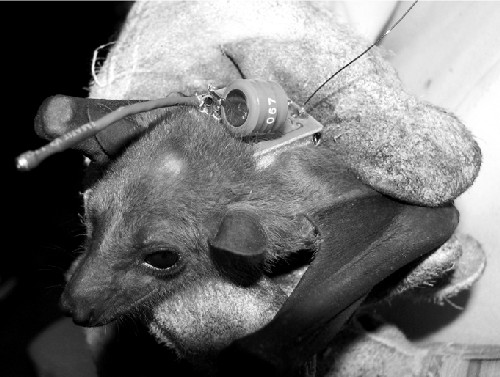
bat
Rousettus aegyptiacus, a type of fruit bat

By James Dacey

Nope, this is not a scheme by the new British government to keep track of mischievous dogs.

This is one of the Egyptian fruit bats involved in research in England and Scotland to unlock the secrets behind bats’ remarkable ability to “see” in the dark.

It is well known that bats use the echoes from their own calls to recreate the landscape through which they are flying.

This is the same basic principle that underpins sonar technology used by submarines to map out the ocean floor and to detect other vessels.

Bats, however, have a super duper version of sonar which enables them to resolve their surroundings in much finer detail. Their two ears receive the echoes at slightly different times and at different loudness levels, depending on the position of the object generating the echoes, enabling them to perceive distance and direction.

Many bats also have an inbuilt acoustic gain control that allows them to emit high-intensity calls without deafening themselves and then to apply a gain to returning signals.

Simon Whiteley at the University of Strathclyde in Scotland has led a team to create a special sensor to monitor this process, which was then mounted onto the backs of a number of Rousettus aegyptiacus.

The six bats performed up to sixteen flights each along a flight corridor. Each flight was short – lasting only about three seconds – but, with the bats’ clicks only lasting a quarter of a millisecond, a large number of calls were recorded for the scientists to analyse.

Back in the lab, the researchers copied the animals’ functions by recreating the bat chirps and receiving them using a spectral equalization technique.

Their findings are published this week in Bioinspiration and Biomimetics.

Whiteley’s team will continue studying these bats with a view to developing applications such as positioning systems for robots.

David Willetts named as UK science minister

By Michael Banks

After a few days of political horse-trading, a resignation speech from former UK prime minister Gordon Brown and the emergence of the first coalition government since the Second World War, the UK has a new science minister.

Last Thursday’s general election resulted in a hung parliament, meaning no party had an overall majority. After days of coalition talks between the three main parties, the Conservatives and the Liberal Democrats joined in a government, with David Cameron as prime minister.

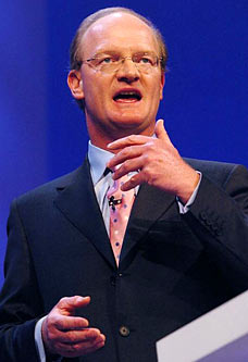
DavidWillettsDM_228x333.jpg

Cameron spent most of yesterday announcing the members of his new cabinet and late last night it emerged that David Willetts, Conservative Member of Parliament for Havant, will be the minister of state for universities and science in the department for business, innovation and skills.

Nicknamed “two brains”, Willetts was shadow secretary of state for innovation, universities and skills from July 2007 and before that was shadow secretary of state for education from December 2005 to July 2007.

Like his predecessor Paul Drayson, who was science minister in the Labour government under Gordon Brown, Willetts will not be a cabinet minister, but will be attending cabinet meetings.

Willetts, however, takes over the role as science minister at a testing time for science funding in the UK. Following the deficit in the budget of the Science and Technology Facilities Council that resulted in the UK pulling out of 25 international projects in December, Drayson won plaudits for making structural changes to the STFC that will better protect the funding council from foreign currency fluctuations that affect its international subscriptions.

Willetts will now have to deal with the ramifications of the STFC’s changes and its continuing budget deficit as well as any budget cuts that could happen when the new coalition government announces its spending review, which is expected to happen in the autumn.

Previous statements by Willetts when he was shadow secretary of state for innovation, universities and skills indicate that he will fight to maintain the science budget from swingeing cuts. “It is important that science is funded properly. It should not be about the government picking winners; it should be about supporting academically excellent research centres,” Willetts said when the STFC’s budget problems first emerged in December 2007. “We will scrutinize these proposals to make sure they improve things after last year’s scandal when the government took £75 million from science by stealth.”

Willetts has also apparently said that he would like to delay the Research Excellence Framework (REF), which is used to allocate funding to individual universities. The REF replaces the Research Assessment Exercise and will include quantitative information like bibliometric data in addition to the existing peer-review evaluation.

The University and College Union (UCU) released a statement today welcoming the appointment of Willetts as science minister. “Mr Willets proved his ability to listen to staff concerns when committing to delay unpopular plans to make university research funding dependent on economic impact,”; says Sally Hunt, general secretary of the UCU. “The academic community made clear its view that assessing and funding research according to its impact is unworkable and we urge him to put an end to this sorry chapter once and for all.”

Hunt also warned that Willetts will need to “listen to the ever-widening consensus of opinion which opposes cuts in college and university budgets, caps on student numbers, the privatization of academic institutions and increases in the cost of a university education for hard-working families”.

The Campaign for Science and Engineering (CaSE) also welcomed Willetts appointment. “In his former roles as shadow secretary for education and then innovation, universities and skills, David Willetts always engaged with science issues,” says Hilary Leevers, acting director of CaSE. “It is vital that the minister for science works closely with the department for education. As former shadow of this department, Willetts will be well positioned to do this.”

DNA robots move with purpose

Two independent teams in the US have made DNA robots mimic the protein motors in our bodies – be it walking without help along predefined routes or taking cargo from A to B.

The experiments, which are the first to truly combine advances in our knowledge of DNA structure and dynamics, suggest that nanorobots could soon be performing autonomous, useful tasks.

“A goal of our field is to re-fashion and re-imagine all the complex biomechanical machinery of cells to suit our own purposes,” says Paul Rothermund, an expert in molecular robotics at the California Institute of Technology who was not involved in the research. “[We want] to have synthetic molecules that can move around, carry cargo, act as chemical factories…and above all to make these processes modular, to make them engineerable. These two papers mark a significant advance along this research direction.”

Walkers and spiders

So far biophysicists have found two ways create such molecular robots. The first, known as DNA walkers, have a body and feet made from DNA, with extra “anchor” strands of DNA that join the feet to a surface. When different “fuel” strands are put in front of a walker, they preferentially join to the anchor strands, thereby freeing the walker to move forward. The second type of robot, known as a molecular spider, has a protein body and DNA legs that chemically cleave tall strands of DNA on a surface. Simply put, a molecular spider nibbles its way through a lawn of DNA, only going where there is more grass to mow.

These two papers mark a significant advance along this research direction Paul Rothermund, California Institute of Technology

But the trouble with these robots is that, in the past, they have only been shown to move slowly and aimlessly. Ideally, researchers would like them to walk in a set direction while performing a meaningful task – rather like Mother Nature’s protein motors, which move along well defined tracks in a cell while carrying cargo.

Now the two research groups – one involving Milan Stojanovic at Columbia University and colleagues, the other led by Ned Seeman at New York University – have got around this problem by exploiting developments in structural DNA, namely “DNA origami”. Based on folded DNA, this neat trick makes something akin to a pegboard to which all sorts of molecules can be attached. In the context of the current research, however, it provides an ideal track for walkers or spiders to move along.

The route to autonomous assembly

Stojanovic’s group have programmed a thin track of DNA origami with a route for a molecular spider. Using an atomic force microscope, they imaged the spider moving forwards in a straight line leaving a trail of cleaved DNA (or cut grass) behind. “An observer, looking at it, could legitimately say that the molecule ‘behaves’ in a certain way, although in reality [the spider] just implements simple leg residency rules,” says Stojanovic.

Seeman’s group, on the other hand, has managed to get DNA walkers to transport cargo. On their origami, the researchers placed three DNA machines that could be set up to donate or keep different types of cargo, so that a passing walker can take on eight (that is, 23) possible loads and deposit them at the end of the track. “This is important because we have combined a number of elements,” explains Seeman. “The walker, the three independently programmed addition stations and the cargo are all sitting on a DNA origami platform. It is the first assembly line built on the nanometre scale.”

The assembly line produced by Seeman’s group might seem a bigger development than the nibbling spider of Stojanovic’s group. But in fact the latter is just as important because the process is fully autonomous. This is unlike the assembly line, which requires the manual addition of DNA fuel strands to keep the walker moving and accepting cargo. The next step might be to create an autonomous assembly line, just like in biology where independent factories, or “ribosomes”, produce different proteins according to the chemical messages they receive.

“Eventually we want to make something as complex as a cell that can have all these independent little factories running in it, each one cranking out a different product based on their program – and this is what Seeman’s paper is starting to show us how to do,” says Rothermund.

The research is reported in Nature .

‘Few-layer’ graphene keeps its cool

The thermal conductivity of multi-layer graphene decreases as the material gets thicker, according to researchers in the US. The team believes that despite the drop, several layers of graphene – sheets of carbon just one atom thick – could be better at cooling tiny electronic devices than conventional copper thermal conductors. The work also confirms a previous study by the group suggesting that graphene conducts heat better than any other known material.

Graphene is a flat sheet of carbon atoms arranged in a honeycombed lattice. It has been attracting the attention of scientists and engineers alike since it was first created in 2004 thanks to its unique electronic and mechanical properties that show great technological promise. In particular, it could be used to make ultrafast transistors because the electrons in graphene travel through the material at extremely high speeds.

In 2008 Alexander Balandin and colleagues at the University of California, Riverside, showed that graphene has a very large intrinsic room-temperature thermal conductivity in the 3000–5000 Wm–1K–1 range, depending on the size and quality of the sample. These values are higher even than diamond, which had been the best heat conductor known.

From 2D to 3D

Until now, however, no-one had studied how the thermal conductivity of multi-layer graphene changes as it goes from being 2D to 3D as more layers are added. Balandin’s team has now done this by measuring the thermal conductivity of “few-layer” graphene samples that contain between two and ten atomic layers. Their non-contact optical technique involves using Raman spectroscopy to measure the local temperature of free-standing graphene flakes.

The researchers found that the material’s thermal conductivity decreases as the number of atomic layers increases. However, it still remains very high at 1300 Wm–1K–1 for graphene containing four atomic layers. By comparison, bulk copper, which is widely used to cool computer chips, has a thermal conductivity of around 400 Wm–1K–1, which decreases to about 250 Wm–1K–1 in very thin copper films.

“In practical applications, graphene needs to be interfaced with composites or other substrates, such as silica (SiO2) chips, which will reduce its thermal conductivity, but the indications are that it will still be better than that of copper,” Balandin told physicsworld.com.

Phonons are at fault

According to the team, the thermal conductivity decreases with thickness because phonons – quantized vibrations of the crystal lattice that transport heat – couple across the different atomic layers in the material. The more layers there are, the greater the coupling and more phonon scattering occurs, disrupting the conduction of heat.

The results confirm that few-layer graphene, which is easier to produce than single layers of the material, could be ideal for removing heat from electronic components, like those used in computer chips. Unwanted heat is a big problem in modern devices that are based on conventional silicon circuits – and the problem is getting worse as devices become ever smaller.

In the short term, according to Balandin, graphene could be used in applications such as thermal interface materials for chip packaging or transparent electrodes in photovoltaics. “However, as the material becomes more widely available in larger quantities in a few years, it might be used in conjunction with silicon in computer chips – for example, as interconnect wiring or as a heat spreader,” he added. The ultimate dream of all-graphene electronics may still be a way off, though researchers around the world are working hard to make it a reality.

Spurred on by these results, the Riverside team is now looking at ways to incorporate few-layer graphene into computer chips.

The work was published in Nature Materials.

Is ball lightning all in your head?

By Hamish Johnston

Ball lightning is a phenomenon in which a fiery sphere floats through the air near the surface of the Earth, usually during a thunderstorm. Or is it?

Although ball lightning is very rare, researchers have collected thousands of eyewitness observations from around the world, and there are even a few photographs of the fiery apparitions. While some researchers have been able to create glowing orbs in the lab, physicists haven’t really been able to explain why they occur in nature.

Well, maybe that’s because ball lightning exists in the brain of the beholder – at least some of the time.

That’s the conclusion of a report recently posted on the arXiv preprint server by Alexander Kendl and Joseph Peer at the University of Innsbruck. They argue that electromagnetic pulses emitted by lightning discharges could lead to the perception of “magnetophosphenes” by persons nearby.

Magnetophosphenes are luminous shapes that are perceived by people undergoing transcranial magnetic stimulation (TMS) – a technique used to stimulate brain activity using magnetic pulses.

Kendl and Peer have calculated that a person up to 100 m away from long-duration (1–2 s) repetitive lightning discharges would receive about the same dose as a TMS subject.

Although they admit that such lightning events are rare, they claim, “Lightning electromagnetic pulse induced transcranial magnetic stimulation of phosphenes in the visual cortex is concluded to be a plausible interpretation of a large class of reports on luminous perceptions during thunderstorms.”

Dungeons and Dragons dice pack densely

From the apples at your local grocery store to the pills in your medicine cabinet, packing products in an efficient manner is an important consideration in many industries. In new research, a group of physicists in the US has investigated the packing properties of a less familiar object, though it may be recognizable to players of the game Dungeons and Dragons – the tetrahedral die. They find that these shapes pack incredibly densely, despite taking on a highly disordered configuration.

Tetrahedra are regular convex shapes possessing four triangular faces. To date very little research has been carried out on how these shapes pack together. But a better understanding of this process could be of interest to geological industries such as oil companies when choosing where to drill their wells. This is because granular matter is more similar to tetrahedra than spheres, which is how it is depicted in basic geological models.

Dense packing

In the past year or so the applied mathematics community has taken up the challenge to investigate tetrahedra, and it has become clear that these shapes could pack much more densely than spheres, at least in theory. In the extensive research on spheres over the years, they have never filled more than 64% of a container, despite a conjecture by Kepler that they could pack to a fundamental limit of 74.05%. In contrast, some recent numerical models have shown that tetrahedra can pack to fractions of more than 85%.

With this latest research, Alexander Jaoshvili at New York University in the US, working with colleagues, has taken a closer look at how tetrahedra pack together in the real world. In a fairly straightforward experiment, the researchers assembled a large number of identical tetrahedral-shaped dice and began adding these to different-shaped containers, shaking and adding more dice until no more could be added. Packing fractions were then determined by injecting a well known filling fluid until the containers were full and subtracting these volumes of fluid from the total volumes of the containers. For one of the large radius containers, a packing density of 0.76 was recorded, which compared with 0.64 for spheres added to the same container.

To probe a little deeper and examine the packing structure, Jaoshvili’s team then placed the packed containers in an MRI scanner. This enabled the researchers to locate the centres of particles and to resolve the kinds of configurations that the dice were taking on. What they saw is that, despite their ability to pack so tightly, the dice are in fact highly disordered within the containers. This finding adds weight to recent theoretical work that suggests that the tetrahedra are aligning themselves into a form of quasicrystal structure upon compression.

All shook up

Jaoshvili and his team were slightly surprised by the disorder. “One would expect that if particles are highly packed they would be highly ordered as well, but with tetrahedrons we find that they are packed with high density and are highly disordered,” says Jaoshvili.

This surprise is shared by Daan Frenkel, a theoretical chemist at the University of Cambridge, who believes that, at the moment, the result can only be explained qualitatively, by comparing tetrahedra with other shapes. “With cubes, the gap-less packing can be continued indefinitely – they can pack 100% of the space. Tetrahedra cannot “tile” space – but they are better at it than spheres.”

Since Jaoshvili submitted his paper there has been a flurry of activity regarding tetrahedral packing and he expects further light to be shed on the quasicrystal structure of the packing in the near future.

This research is published in Physical Review Letters.

Copyright © 2026 by IOP Publishing Ltd and individual contributors