Web life: Trailblazing

So what is the site about?

This year marks the 350th anniversary of the founding of the Royal Society, the world’s oldest continuously existing learned society. Since its beginnings in 1660 as a “College for the Promoting of Physico-Mathematical Experimental Learning”, the society has published some 60,000 papers in disciplines from physics to biology, spread over a handful of different journals. Trailblazing brings the daunting scale of this archive down to size with an interactive timeline of 60 papers, carefully selected to reflect the society’s history. Written by luminaries such as Newton, Faraday and Dirac along with lesser-known scientists, all of the papers are available to download free of charge, and each one is prefaced by comments from current scientific experts.

Can you tell me about some of the papers?

Readers will find a little bit of everything in this timeline, which begins with some rather cringe-worthy medical experiments from the late 1660s and continues through to a 2008 entry on geoengineering. Most of the papers are in English, although Alessandro Volta’s 1800 description of the construction of an electric battery is written in French. Among the other physics and astronomy entries, be sure to check out Newton’s 1671 paper containing his “New Theory about Light and Colors”, the 1752 account of Benjamin Franklin’s famous kite-flying investigations and Egon Orowan’s 1938 explanation of metal fatigue. This last paper covers an industrially important phenomenon first spotted by railway engineers more than a century before Orowan, a Hungarian-born physicist then based at Birmingham University in the UK, succeeded in describing it mathematically. While Orowan’s breakthrough may not be in the same league as, say, Maxwell’s unification of electricity and magnetism, it is nevertheless worthy of inclusion. History, after all, is made by good scientists as well as great ones.

What are some other highlights?

The earliest years of the timeline are an antiquarian’s dream, complete with archaic spellings and those elongated letter s’s that look like f’s. It is, however, amusing to see how little some other things have changed since then. In Edmund Halley’s report on the lunar eclipse of 1715, he notes with regret that “my worthy Colleague Dr. John Keill by rea∫on of Clouds ∫aw nothing di∫tinctly at Oxford but the End”. Intriguingly, it seems that Keill’s Cambridge counterpart Roger Cotes had other things on his mind that night – Halley delicately suggests that Cotes “had the misfortune to be oppre∫t by too much Company, ∫o that, though the Heavens were very favourable, yet he mi∫s’d both the time of the Beginning of the Eclip∫e and that of total Darkne∫s”. (Ah, those naughty academics!) Reading such delights online is not quite the same as reading them in the original manuscripts. However, the Web versions are a lot easier to find, and there is even a link where you can sign up to receive free e-mail alerts when new articles cite the timeline articles – although in Halley’s case, this seems unlikely.

What can I learn from the timeline as a whole?

One of the most striking trends that emerges when you look at papers from different eras is the gradual professionalization of science. In the early years of the Royal Society, for example, astronomical observations were mostly being performed by amateurs. By the time Norman Lockyer reported his 1898 discovery that the Sun’s corona is much hotter than its surface, the Reverend Whoevers and Lord Thingummies cited in Halley’s time were almost entirely replaced by Professor So-and-sos. The level of technical detail also increases dramatically. Funny letter s’s notwithstanding, any literate person could read Franklin or Faraday and understand exactly what these pioneers were doing – not least because technical diagrams were, it seems, rather more clearly labelled in the 18th and 19th centuries. Tellingly, the most recent pure-physics paper selected for inclusion in the timeline is Stephen Hawking and Roger Penrose’s 40-year-old work on black holes, but there is still hope for the future: the timeline stretches as far as 2050, and there is plenty of space for new entries.

That’s hella signatures

100bNote.jpg
0.0000000000000001 helladollars?

By Michael Banks

“Yotta”, “zeta”, “exa” and “peta” could now be joined by a new number prefix, the “hella”, if a physics student from University of California, Davis, gets his way.

Austin Sendek has started a petition on the social networking site Facebook to establish a new, scientifically accepted prefix for 1027(that is 1 followed by 27 zeroes, or 1000000000000000000000000000).

Yotta (1024), which was established in 2001, is currently the largest number established in the International System of Units (SI) – the world’s most widely used system of measurement — with zeta (1021), exa (1018) and peta (1015) following close behind.

“Hella” comes from Californian slang for “very” or “a lot of”. Sendek says that by accepting the term the SI system can “not only rectify their failing prefix system but also honor the scientific progress of Northern California.”

The petition is gaining ground fast with over 20 0000 signatures (or “fans” on the Facebook page) – or 0.0000000000000000000002 hellafans.

So what could you use the hella for? Sendek claims it could be applied in many “crucial calculations”, including the wattage of the Sun (0.3 hellawatts), or the number of atoms in a large sample (6.02 hellaatoms in 120 kg of carbon-12).

Sendek has not said what he would like to call the number for 10-27 (10-24 is the yocto). So physicsworld.com readers, any suggestions?

Junctionless transistor makes its debut

Researchers in Ireland have succeeded in making the first junctionless transistor ever. The device, which resembles a structure first proposed way back in 1925 but not realized until now, has nearly “ideal” electrical properties, according to the team. It could potentially operate faster and use less power than any conventional transistor on the market today.

Transistors are the fundamental building blocks of modern electronic devices – and all existing transistors contain semiconductor junctions. The most common type of junction is the p–n junction, which is formed by the contact between a p-type piece of silicon – doped with impurities to create an excess of holes – and an n-type piece of silicon, doped to create an excess of electrons. Other junctions include the heterojunction, which is simply a p–n junction containing two different semiconductors, and the Schottky junction between metal and semiconductor.

The number of transistors on a single silicon microchip has been increasing exponentially since the early 1970s, and has gone up from a few hundred to over several billion today. As a result, transistors are becoming so tiny that it is becoming increasingly difficult to create high-quality junctions. In particular, it is very difficult to change the doping concentration of a material over distances shorter than about 10 nm. Junctionless transistors could therefore help chipmakers continue to make smaller and smaller devices.

Patented in 1925

Now, Jean-Pierre Colinge and colleagues at the Tyndall National Institute of University College Cork have dispensed with the very idea of a junction and instead have turned to a concept first proposed in 1925 by Austrian-Hungarian physicist Julius Edgar Lilienfield. Patented under the title “Device for controlling electric current”, it is a simple resistor and contains a gate that controls the density of electrons and holes, and thus current flow.

The team’s version of the device consists of a silicon nanowire in which current flow is perfectly controlled by a silicon gate that is separated from the nanowire by a thin insulating layer. The structure itself is very simple, looking a bit like a telephone cable that is fixed to a surface by a plastic clip (see figure). Crucially, there is no need to alter the doping over very short distances. Instead, the entire silicon nanowire is heavily n-doped, making it an excellent conductor. However, the gate is p-doped and its presence has the effect of depleting the number of electrons in the region of the nanowire under the gate.

If a voltage is simply applied along the nanowire, current cannot flow through this depleted region. According to Colinge, this region “squeezes” the current in the nanowire in the same way as the flow of water in a hose is stopped by squeezing it. However, if a voltage is applied to the gate, the squeezing effect is reduced and current can flow. The team also made a similar device with a p-type nanowire and n-type gate.

The most perfect of transistors

The structure is simple to build, even at the nanoscale, which means reduced costs compared with conventional junction fabrication technologies, which are becoming more and more complex. The device also has near-ideal electrical properties, adds Colinge, and behaves like the most perfect of transistors. This means that it hardly suffers at all from current leakage – the bane of conventional devices – and so could potentially operate faster and using less energy.

The Tyndall team says that it is now talking to some of the world’s leading semiconductor companies to further develop and possibly license its technology.

“Although the idea of a transistor without junctions may seem quite unorthodox, the word “transistor” does not imply the presence of junctions, per se,” write the researchers in Nature Nanotechnology, where the work was published. “A transistor is a solid-state device that controls current flow and the word transistor is a contraction of ‘trans-resistor’.”

Both answers correct in century-old optics dilemma

For 100 years physicists have been struggling to reconcile two different formulations describing the momentum of light travelling through a transparent medium. One, put forward by German mathematician Hermann Minkowski in 1908, stipulates that light’s momentum increases when it enters a medium, while the other, advanced a year later by the German physicist Max Abraham, instead says that the momentum of light decreases. Now, Stephen Barnett of the University of Strathclyde in the UK has concluded that both formulations are in fact correct, with the difference essentially boiling down to whether one considers the wave or particle nature of light.

It is well known than when light enters a material medium it slows down in proportion to the refractive index, n, of that medium. Minkowski and Abraham wanted to know how light’s momentum changes as a result. Abraham calculated that the momentum of a single photon within the light is also reduced by a factor n, a result which agrees with our experience of everyday objects – as their speed drops, so too does their momentum. Indeed, a number of powerful arguments have been put forward over the years in support of this position. Prominent among these has been a simple proof based on Newton’s first law of motion and Einstein’s equivalence of mass and energy, which considers what happens when a single photon travels through a transparent block and transfers some of its momentum to the block, given that the motion of the system’s centre of mass-energy must remain constant.

Minkowski’s formulation, on the other hand, seems more natural from the point of view of quantum mechanics. As light slows down inside a medium its wavelength also decreases, but quantum mechanics tell us that shorter wavelengths are associated with higher energies, and therefore higher momenta. In fact, Minkowski’s approach suggests that the momentum of a single photon of light increases by a factor n as it passes through a medium. This result can also be supported by strong theoretical arguments, among them one that considers what happens when an atom moving at some speed through a medium absorbs a photon and experiences an electronic transition.

Fundamental physical principles at stake

As Barnett points out, this problem has kept physicists interested for so long because it appears to put one or more fundamental physical principles at stake – on the one side Newton’s first law and Einstein’s famous E = mc2 and on the other the notion, familiar from de Broglie waves, that momentum is inversely proportional to wavelength.

These two formulations reflect the fact that in different situations momentum does different things Stephen Barnett, University of Strathclyde

Both formulations have received experimental support, particularly that of Minkowski. For example, in 2005 Wolfgang Ketterle and colleagues at the Massachusetts Institute of Technology reported evidence in favour of Minkowski by transferring momentum from laser beams to matter waves that had been formed from a few million atoms cooled to just above absolute zero. However, in 2008 a group led by Weilong She of Zhongshan University in China passed a laser beam through a tiny filament of silica and found that the filament recoiled as the light exited, indicating, in accordance with Abraham, that the light gained momentum as it left the material.

According to Barnett, however, both formulations are correct. He says that the one put forward by Abraham corresponds to a body’s “kinetic momentum” – its mass multiplied by its velocity. Minkowski’s momentum, on the other hand, is a body’s “canonical momentum” – Planck’s constant divided by its de Broglie wavelength. “These two formulations reflect the fact that in different situations momentum does different things,” he adds. “In free space they coincide, but not when inside a medium.”

Don’t mix up the two

Physicists have known for some years that this distinction might explain the dilemma but have been unable to prove it. That is to say, they have been unable to reconcile the two different formulations with electromagnetic theory. Barnett overcame this problem when he realized that the two approaches cannot be treated in the same way mathematically – that of Abraham requires considering momentum as transferred by individual particles whereas that of Minkowski instead involves the commutation relationship between momentum and position, a wave property. “It is when you mix the two up that you get the problem,” he says.

The question is: when is the particle momentum relevant and when is the wave momentum relevant? Ulf Leonhardt, University of St Andrews

This point is underlined by Ulf Leonhardt of the University of St Andrews in the UK, who says that, simply put, Abraham described the momentum of light as a particle whereas Minkowski described the momentum of light as a wave. As such, he agrees that both formulations are correct. However, he does not think that the debate is really over. “The question is: when is the particle momentum relevant and when is the wave momentum relevant? Are there cases when a mixture of wave and particle properties appear?” he asks. “When science answers one question, ten new questions appear.”

Barnett is also not entirely satisfied. “We now know that Abraham and Minkowski were both right,” he says. “But we don’t yet know why nature requires two momenta.”

The work is reported in Phys. Rev. Lett. 104 070401.

What Rutherford may have left behind

rutherford.jpg

By Hamish Johnston

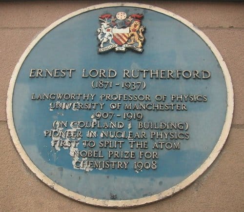
Did the leftovers from experiments done by Ernest Rutherford and others contribute to the deaths of two University of Manchester academics nearly a century later?

That’s the question facing Manchester coroner Nigel Meadows, who will lead an inquest into the deaths of Arthur Reader and Tom Whiston, who both died of pancreatic cancer in 2008 and 2009 respectively.

Rutherford arrived at the University of Manchester in 1907 and spent the next 12 years experimenting with radioactive materials as well as toxic substances such as mercury. It was there that he established the existence of the atomic nucleus.

Rutherford’s lab was in the New Physical Laboratories (renamed several times before it became the Rutherford building in 2006), which continued to be used by the physics department until the late 1960s. The psychology department moved there in 1972 — but staff only discovered that something was wrong in 2001 when several rooms were sealed off because of radiation and mercury contamination.

In 2008, three psychologists and longtime occupants of the building published a 294-page report entitled Possible health risks due to ionising radiation in the Rutherford Building.

In their report, John Churcher, Don O’Boyle and Neil Todd conclude:

“There remains significant uncertainty concerning the extent to which radioactive
contamination of the Coupland 1/Rutherford building may have affected the health of
staff of the Department of Psychology who occupied part of it during the 25 years to
1999 and the health of others who occupied it earlier.

However, in 2009 the epidemiologist David Coggon of Southampton University tabled an independent report that concluded the deaths (as well as the health problems of several other occupants) were probably not linked to the contamination. You can read Coggon’s report here.

It will be interesting to see how the coroner’s findings compare to previous investigations.

Hail the first sound ‘lasers’

Two independent groups of physicists have unveiled the first phonon “lasers” – devices that emit coherent sound waves in much the same ways as lasers emit coherent light waves. Sometimes called “sasers”, one of the devices emits sound at about 400 GHz while the other operates in the megahertz range.

Such very high frequency sound could be used to probe the interiors of tiny objects – and the ability to create laser-like beams of sound could lead to new imaging applications. Indeed, the differences between the two devices suggest that sasers could be made to operate over a wide range of frequencies.

At the heart of any optical laser is a medium with an electronic transition that involves the emission of a photon. The medium is “pumped” by an external energy source so that the majority of the electrons are in the higher energy state of the transition. When such a state decays, it emits a photon that can stimulate the emission of many more photons – which in turn stimulate further emission. Because they are all produced by the same quantum process, the photons emerge as a coherent beam of light.

Spontaneous emission problems

Just as light behaves as both particle and wave, so sound can be described in terms of particles called phonons – quanta of vibrational energy that behave in much the same way as photons. While there is no reason why stimulated emission shouldn’t also work for phonons, physicists had struggled to find materials in which stimulated emission – rather than random spontaneous emission – is the dominant decay process.

Now, two independent groups have come up with two very different solutions to this problem.

At the University of Nottingham in the UK, Tony Kent and colleagues have made a saser that operates at about 440 GHz. Their device comprises alternating layers of the semiconductor gallium arsenide (GaAs) and the insulator aluminium arsenide (AlAs). The GaAs layers act as quantum wells, which can trap electrons. If an electrical bias is placed across the layers, the electrons are inclined to hop across an AlAs barrier into the next well – emitting a phonon in the process. Crucially, such a hop can be stimulated by a similar phonon. To ensure that the phonons bounce back and forth through the structure like photons in a laser cavity, the team set the distance between the repeating layers to resonate with the wavelength of the phonons.

The team tested the device by firing a femtosecond laser pulse at one end of the layered structure. This creates phonons that initiate the stimulated emission. A second laser pulse is then bounced off the device to measure the reflectance of the material over several hundred picoseconds. Kent and colleagues observed oscillations in the reflectance that are caused by coherent phonons.

As the team increased the bias voltage from 80–180 mV, it saw an increase in the amplitude of the coherent phonons that peaked at about 160 mV before falling at higher voltages. According to Kent, the peak occurs when the phonon wavelength resonates with the device.

Pair of resonators

Meanwhile at the California Institute of Technology (Caltech), Ivan Grudinin and colleagues use two microwave resonators – each about 6 µm in diameter and made of silica – to create the phonon-producing transition for their saser. The resonators are separated by a gap of about 1 µm, which is small enough for the devices to be coupled via light waves to form a two-state quantum system.

A laser is used to pump the system to the higher energy state. Phonons at megahertz frequencies are emitted, stimulating the further emission of phonons. The team confirmed that the system was indeed a phonon laser by turning up the pumping power and observing no sound emission until a threshold level – above which the power increased rapidly and sound was emitted in a very narrow frequency range.

Kent told physicsworld.com that the two approaches are complementary and it should be possible to use one device or the other to create coherent phonons at any frequency in the megahertz to terahertz range.

Probing nanotechnology

A terahertz saser would be particularly useful in nanotechnology because its phonons would have a wavelength of about one nanometre and could penetrate relatively deep into a solid structure – opening the door to 3D imaging of nanostructures. This is unlike current analysis techniques such as electron microscopy, which are limited to surface analysis.

Sasers could also be used to cause the periodic strain of a material – modulating its optical or electrical properties. This could be used to create very fast switches or to generate terahertz electromagnetic radiation – something that is currently difficult to do.

“The next step is to optimize the device to increase the coherent acoustic output and minimize the background from spontaneous emission,” said Kent. “We are also working on devices that can be integrated with a saser to make a kind of acoustic lab on a chip to measure nanostructures.”

The devices are described in Phys. Rev. Lett. 104 083901 and Phys. Rev. Lett. 104 085501.

Stamping your mark on science

Royal Society Stampcard 8.jpg
One of 10 Royal Mail stamps celebrating 350 years of the Royal Society

By Michael Banks

Physicist Ernest Rutherford – famous for his model of the atom in 1911 — once said that “All science is either physics or stamp collecting.”

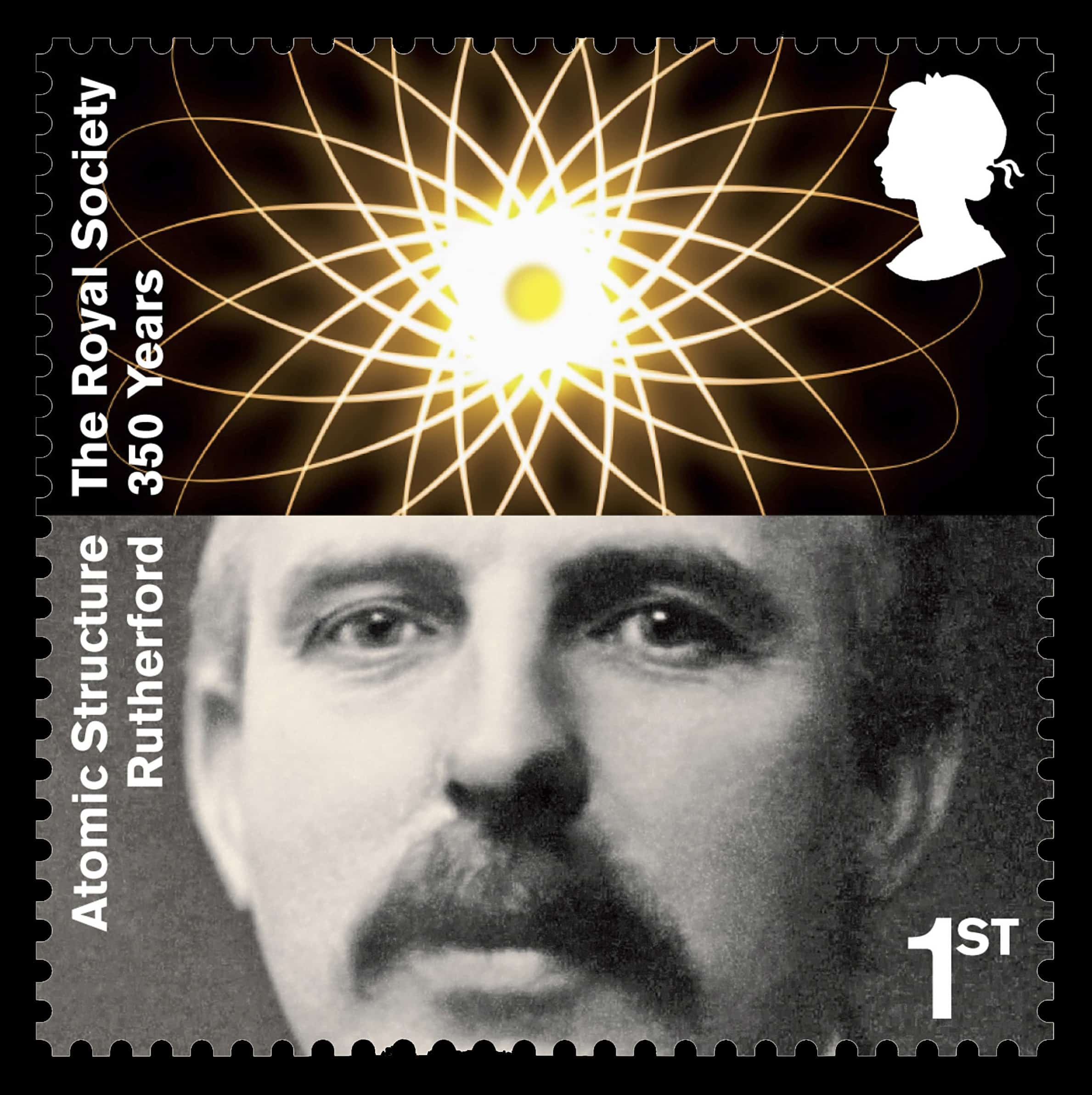
But for all you stamp-collecting physicists out there you can now get your hands on 10 stamps launched today by the Royal Mail to celebrate 350 years of the Royal Society.

Featuring luminaries such as Isaac Newton, Benjamin Franklin and Robert Boyle, the first-class stamps are apparently the first to contain a “split-stamp” design (could it be a reference to Rutherford’s “splitting the atom” experiments in 1917?) — the portraits of the 10 fellows are each paired with a colourful image representing their achievements.

Royal Mail selected the 10 pioneering scientists with the help of the Royal Society and you can get your hands on the stamps by visiting any Post Office in the UK or online at www.royalmail.com/stamps

Crystal control moves towards 3D displays

In a step towards futuristic 3D-display screens, researchers in Singapore have found a simple way to control the growth of tiny crystals that have useful optical properties. By careful doping with lanthanide elements, the researchers found that they could adjust the crystal structure, size and emission spectra of sodium yttrium flouride (NaYF4).

Known as “upconversion nanocrystals”, NaYF4 crystals could play a critical role in the development of 3D-display technology, as they absorb near-infrared light and emit visible light. One promising application is dispersing them in transparent silicone displays, where infrared lasers can be used to generate images in 3D by scanning the silicone with invisible light causing the appropriate nanocrystals to emit visible light.

In addition, because NaYF4 is nontoxic and biocompatible, there is great potential for advanced bioimaging or luminescent biological labelling. Using near-infrared radiation for these applications is safer and more accurate than using ultraviolet light.

But to be effective at upconversion, the crystals need to be less than 20 nm in size and have a hexagonal crystal structure. Achieving this has proven challenging, because small NaYF4 crystals naturally favour the cubic crystal structure. Conversion to the hexagonal form typically requires harsh chemical reagents or prolonged heat treatments – conditions that can lead to other problems, such as the crystals sticking together or changing in size.

Doping decision

Now, Xiaogang Liu and colleagues at the National University of Singapore have found a much simpler way to control the growth of these crystals: by introducing carefully controlled quantities of lanthanide ions into the structure. Adding small amounts of heavy elements in this way is usually referred to as “doping” and is commonly used to make hybrid materials with unusual or desirable properties.

“We have discovered a new nanocrystal growth phenomenon induced by lanthanide doping,” Liu told physicsworld.com. ‘This allows us to control which phase the crystals grow in, but also adjust other properties. We can control the size of the nanocrystals – from several hundred nanometres to ten nanometres – but also fine tune the colour of their emissions from green to white and blue.’

The team first discovered that adding small amounts of gadolinium during crystal formation encouraged the crystals to form in the desired hexagonal phase. This takes place as some gadolinium ions take the place of yttrium ions, producing crystals of NaGdF4 mixed in with NaYF4. The presence of these crystals is thought to direct the rest to form in the hexagonal phase.

Lanthanide hunt

The team then explored other lanthanides, identifying that samarium and neodymium doping produced smaller crystals, while erbium, ytterbium and thulium doping changed the colour of the visible light that was emitted. Liu hopes that, with further research, optimized combinations can be found that will lead to other nanocrystals with different desirable properties.

This research is very interesting and can potentially open up new ideas in controlling nanomaterial growth Song Jin, University of Wisconsin

“This is a new concept in materials science, and a fundamental discovery rather than simply a synthesis technology – although it is a more efficient way to make small nanocrystals than conventional methods,” Liu says. “We will continue to explore the technological applications of these nanocrystals in photodynamic therapy, bioimaging, and animated 3D colour displays.”

Song Jin, a nanocrystals expert at the University of Wisconsin in Madison first heard about the work during a visit to Singapore in January. “This research is very interesting and can potentially open up new ideas in controlling nanomaterial growth. What intrigues me personally the most is that how the addition of dopants changes so much of the crystalline phase and morphology of the nanostructures.”

The study is described in Nature 463 1061.

Making sculptures that move


Why did you choose to study physics?

My interest in science started very early, probably with science-fiction books like the Tom Swift series, which are aimed at children. After brief stints in chemistry and engineering, I chose to study physics at Boston University because I found it the most challenging. I also had dreams of being an “inventor” and thought physics would give me an understanding of how things worked.

How did you become interested in sculpture?

Towards the end of my degree, I started spending time at the Rhode Island School of Design, where my future (and present!) wife Marji was studying sculpture and art education. The world of art was new to me, and I was particularly fascinated by some static wooden machine sculptures she had constructed. I kept suggesting that she make them move but she was not interested and suggested I try instead. After I graduated in 1974, I started working as a computer programmer for an insurance company. It was a tedious job that involved long periods of waiting, so during those downtimes I started sketching ideas for small kinetic toys. I left the programming job after nine months and started Wood That Works by selling these toys at local craft fairs. The toy designs evolved into the first kinetic wall sculptures. I had found a way to invent, but it was in an area I had never dreamed of.

How are your sculptures constructed?

All of my work is driven by constant-force springs, which use a two-spool set-up where a stainless-steel spring band is wound from one spool back against its natural coil direction onto a second spool. As the spring fights to return to its original form, it provides a fairly even torque over the full length of the band. This mimics the torque provided by a traditional clock-weight drive, but in a more compact form. The concept of a constant-force spring confuses many people, because they think of it as a constant-velocity spring motor – something that will turn a wheel at a constant rotational speed. That is not the case: the torque or force is constant, but the unregulated rotating wheel will just keep accelerating until the spring is fully unwound – often creating quite a mess!

So from a purely mechanical view, my sculptures are devices that regulate the unwinding of a spring. Over the years, I have invented quite a few different mechanisms to do this, starting with the concept of clock escapements and extending it to create longer, more active action cycles and random motion. I have two major advantages over clock designers: my works do not have to run for days and they do not have to keep time. Instead, my goal is to create interesting patterns of motion that keep moving (and entertaining) for hours.

How does your training in physics help?

It is essential to my career as a kinetic sculptor. Knowledge of basic mechanics is a necessity, but the analytical study and problem-solving skills that I developed as a physics student have been, if anything, far more important. The intense initial design period when I was visualizing the concept of spring-driven kinetic sculptures felt very much like the long days and nights at university when I tried to get my head round advanced physics concepts.

www.woodthatworks.com

'Subtle defect' worry at LHC

By Hamish Johnston

joint.jpg
Something to worry about: brown bars are the copper stabilizers

A few weeks ago Matthew Chalmers reported that Higgs-hunting particle physicists will have to wait until 2013 before the LHC reaches its maximum energy.

The nuts and bolts of why are described nicely in a new paper called Superconductivity: its role, its success and its setbacks in the Large Hadron Collider of CERN, which has just been published in Superconductor Science and Technology.

The paper — by CERN’s Lucio Rossi — includes a section called “Incident in sector 3-4” that describes in great detail the accident that took down the LHC in 2008. You can read exactly how an electrical connector failed — vaporizing a length of superconducting cable, heating the surrounding helium, which surged along the beam line wreaking havoc.

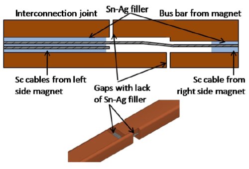
Could a similar disaster strike again? Rossi appears to say yes — “…a more subtle defect, related to a lack of continuity in the copper stabilizer, is now evident and is worrying since it is diffused around the machine”.

These copper stabilizers are part of an electrical circuit used to divert current from the superconducting cable if a fault occurs. Rossi is worried because at some connectors there is insufficient electrical contact between the cable and stabilizers — and between adjacent stabilizers. In the diagram above this trouble spot is labelled “Gaps with lack of Sn-Ag filler”.

If such a splice between cables fails — as one did in 2008 — the adjacent cable is heated and is no longer superconducting. If the cable is bare and there is a gap between stabilizers, current is forced to flow through the cable causing it to melt in a matter of seconds.

While the LHC has implemented a new system for detecting bad splices before they can cause damage, Rossi says that the gaps at the connectors could themselves be a problem. Warm helium from a minor problem elsewhere could, for example, heat the connector — triggering a similar disaster as occurred in 2008.

LHC scientists have devised a way of finding such gaps — but it works best when the LHC is warm. Half the accelerator was warmed up in 2008 for repairs and gaps were found and fixed. Most of the other half, however, was kept at 80 K and could not be thoroughly tested and repaired. As a result, Rossi believes that several gap defects could remain in the accelerator.

The upshot is that CERN will run the LHC in 2010 at the lower energy of 7 TeV, hoping that the connectors will hold. Then the accelerator will be shut down in 2012 for a year so all 10,000 connectors can be replaced. Finally, in 2013 protons in the LHC will collide at 14 TeV.

But the paper is not all bad news — it also describes how the LHC is at the pinnacle of superconducting technology. Here are a few superlatives:

– The accelerator has nearly 10,000 superconducting magnets

– The magnets are cooled by 130 tonnes of helium held at 1.9 and 4.2 K

– The accelerator contains about 15,000 MJ of magnetic energy

– 1200 tonnes of Nb-Ti superconducting cables were used to wind the magnets

– There is a 0.01% variation in field quality among the 1232 main dipole magnets

Copyright © 2026 by IOP Publishing Ltd and individual contributors