Mapping the uptake of glucose in the brain and body provides clinicians with information about the metabolic dysfunction observed in conditions such as cancer, diabetes and Alzheimer’s disease. This mapping is traditionally performed by administering radioactive substances that act as glucose analogues and can be visualized on medical images.
Scientists know, for example, that tumour cells gobble up glucose more than normal cells. Clinicians exploit this by using 18F-FDG-PET imaging to diagnose and localize tumours and to evaluate treatments. This imaging technique, however, cannot assess downstream metabolites that may be important for diagnosis and treatment evaluation – and it also requires injecting the patient with a radioactive compound.
Another technique, magnetic resonance spectroscopy (MRS) with carbon-13, can quantify downstream metabolites but cannot precisely localize them. Meanwhile, the emerging technique of hyperpolarized 13C-MRS imaging does not provide information about some downstream metabolites, including glutamate and glutamine. Hyperpolarized 13C-MRS imaging also requires injections and uses specialized hardware that may not be available in clinical settings.
Researchers at the Medical University of Vienna have now developed a new approach to mapping glucose metabolism. The technique doesn’t rely on radiation or injections but instead uses clinically-available magnetic resonance imaging (MRI) and oral ingestion of a glucose solution.
2H-MRS
In the researchers’ initial validation study, which appears in Investigative Radiology, participants were imaged with 3 T MRI after fasting overnight and again after ingesting deuterium-tagged glucose solution (deuterium, a stable isotope of hydrogen, is not radioactive). The 2H-MRS scan included a 3D echoless free induction decay sequence, and water suppression was performed using conventional water suppression scheme. After the MRS scan, a 3D T1-weighted magnetization-prepared rapid gradient echo readout scan was performed. An in-house software pipeline was used to process data.
The 2H-MRS imaging approach allowed the researchers to quantify oxidative and anaerobic glucose utilization and assess neurotransmitter synthesis. Yet, they could only measure a limited number of deuterated compounds, and specialized hardware was needed to perform the imaging. So they conducted a follow-up study – now published in Nature Biomedical Engineering – to see whether proton MRS (1H-MRS) at 7 T would provide higher sensitivity, chemical specificity and spatiotemporal resolution than 2H-MRS imaging.
1H-MRS
Studies in animals have shown that deuterium-labelled glucose is readily taken up by brain cells, and deuterons are incorporated into downstream glucose metabolites. Because deuterons substitute protons in the molecule, they do not contribute to the proton spectrum, thus an increase in deuterium-labelled metabolites is reflected by a decrease in metabolite signals in 1H-MRS.
In the 1H-MRS study, five participants (four males and one female) received the deuterium-labelled glucose solution, and their blood glucose levels were measured several times over 90 min. The researchers quantified glutamate, glutamine, γ-aminobutyric acid and glucose deuterated at specific molecular positions. They also mapped deuterated and non-deuterated metabolites. They note that the imaging technique does not require specialized hardware to work with clinically available systems.
Fabian Niess, a research associate involved with the Nature Biomedical Engineering study and lead author of the Investigative Radiology study, explains in a press release that the Investigative Radiology study was “an important step” to demonstrate that the approach worked on lower-field systems “because 3 T MR systems are extremely widespread in clinical applications”.
The researchers conclude that 1H-MRS imaging may facilitate glucose metabolism studies, and they are conducting additional research to verify their approach and preliminary results.
One of the world’s leading trade fairs to be devoted to all types of laser and photonic technologies will take place on 27–30 June 2023 in Munich, Germany. LASER World of PHOTONICS will bring together thousands of delegates from all over the world to explore the latest innovations in photonics components and systems, as well as how they are being exploited in novel applications.
More than 1200 companies will be featured at the exhibition, with key industry sectors ranging from industrial manufacturing and energy technologies through to biophotonics and data processing. Other focal points for the exhibition will be light-based sensors, test and measurement solutions, as well as imaging solutions and integrated photonics.
This year’s event will once again feature a dedicated platform for quantum technologies. World of QUANTUM aims to make connections between leading suppliers of photonics equipment and quantum developers working across applications in sensing and imaging, computing and secure communications systems.
Running alongside the exhibition will be the World of Photonics Congress, which includes several thousand presentations across seven specialist conferences. A complementary programme of industry forums, panels and round-table discussions will also offer an expert insight into the commercial trends and emerging applications within the photonics sector.
Read on to find out more about some of the companies and product innovations that will be featured at the show.
Spectrometers combine speed with performance
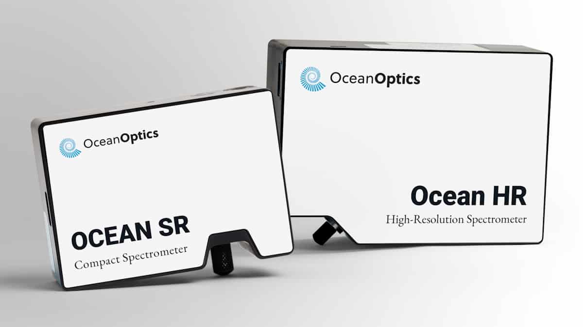
Ocean Optics, a brand of Ocean Insight, will be introducing two new families of spectrometers at this year’s LASER World of Photonics. First up is the Ocean HR series of compact, high-resolution spectrometers, which offer fast acquisition speeds along with excellent thermal wavelength stability and low stray light to enable reliable performance in demanding environments.
Fast and versatile: two new ranges of spectrometers from Ocean Optics have been optimized to meet different performance criteria. (Courtesy: Ocean Optics)
The HR series comes in three different models to meet the specific measurement requirements of different applications. The HR2 combines the fastest acquisition speed with a high signal-to-noise (SNR) ratio, making it ideal for laser and LED characterization, while the HR4 provides high optical resolution for applications such as identifying narrow-band emission peaks in plasmas. Meanwhile, the HR6 combines high resolution with high sensitivity to ultraviolet light, enabling precise measurements of UV absorbance in solutions and gases.
The other new addition is the compact and versatile Ocean SR series of spectrometers, which combine fast acquisition speeds with a high SNR. These multi-use instruments can be exploited for applications ranging from measuring distinct spectral peaks in plasmas and emission sources to detecting subtle absorbance changes in DNA, proteins and other biological samples, and are also well suited for integration into customized systems for high-volume industrial and OEM applications.
Different models have again been optimized for different measurement requirements, with the SR2 combining speed with high SNR, SR4 offering high resolution, and SR6 delivering high sensitivity. Both series of spectrometers can be coupled to Ocean Optics’ light sources, accessories and software, and are supplied with OceanDirect, a cross-platform Software Developers Kit that allows users to optimize spectrometer performance, access critical data for analysis, and exploit a hardware-accelerated signal-averaging tool to improve the SNR performance.
Visit Ocean Optics at booth 421 in Hall A3 to discuss your measurement requirements.
Optical encoder sets new standards for motion control
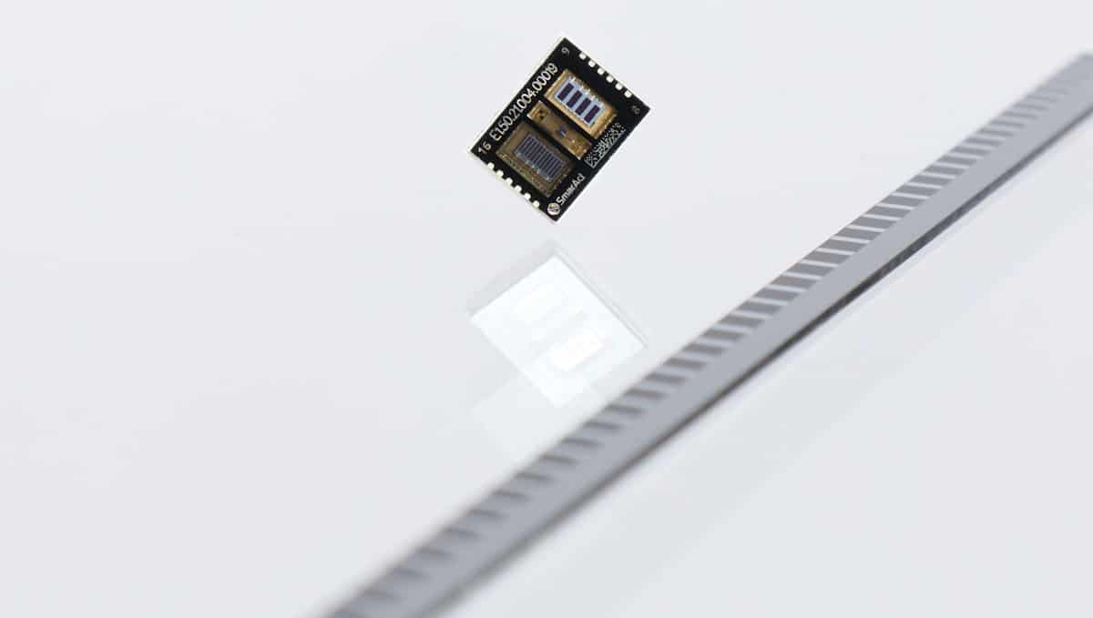
The METIRIO encoder from SmarAct Metrology, part of the SmarAct Group that produces state-of-the-art solutions for positioning, metrology and automated micro-assembly, exploits the latest optical sensor technology to deliver exceptional accuracy and reliability in a compact package. Designed to meet the demands of today’s precision motion-control systems, the encoder can be used in applications ranging from robotics and automation through to semiconductor manufacturing and aerospace.
Precision control: the METIRIO optical encoder from SmartAct provides an accurate, reliable and compact read-head for precision motion-control systems. (Courtesy: SmartAct)
The advanced optical design exploited in the encoder provides excellent signal stability and insensitivity to environmental noise, ensuring consistent performance and smooth motion control even in demanding industrial environments. Its robust construction and reliable operation ensure consistent performance and a long life, reducing both maintenance costs and system downtime.
The encoder has a compact form factor and flexible design, allowing easy integration into a wide range of motion-control systems, while advanced signal processing algorithms are used to optimize the signal quality and its stability. By offering a new level of precision and reliability, the encoder enables companies to optimize their processes, increase productivity and improve overall operational efficiency.
“The METIRIO encoder has fundamentally changed the field of motion control,” said Sebastian Rode, CEO of SmarAct Metrology. “This revolutionary encoder has proven to be very reliable and has been well received. It underscores our commitment to delivering innovative solutions that meet the evolving needs of our customers to achieve superior performance in their motion control applications.”
To find out more about the METIRIO encoder, visit SmarAct at booth 107 in Hall B2.
Wireless solution enables remote monitoring of high-power lasers
Gentec-EO, which specializes in developing solutions for laser beam and terahertz source measurement and analysis, will be demonstrating its HP-BLU series of wireless detectors for the remote monitoring of high-power lasers operating at up to 15 kW. The detectors allow the laser power to be measured at distances of up to 30 m away from the point of delivery, providing safe and accurate monitoring of multi-kilowatt laser systems that are typically confined in an enclosure or operated from another room.
Safe and accurate: the HP-BLU series of wireless detectors from Gentec-EO enable remote measurement of high-power laser beams. (Courtesy: Gentec-EO)
Standard models are available for laser powers of up to 4, 12 and 15 kW, and offer an effective aperture of up to 125 mm to accommodate the largest laser beams. Customized versions are also available to handle higher output powers, or to provide larger apertures with different shapes.
The detectors are equipped with an integrated wireless data-transfer module that transmits all the laser measurement data direct to a PC. Battery operation also avoids the need for additional cabling, reducing the risk of accidents in the workspace.
To find out more, visit Gentec-EO at booth 319 in Hall B2.
Gratings and spectrometers tackle demanding applications
Wasatch Photonics has reoptimized its line of VPH transmission gratings and spectrometers to meet the needs of researchers and OEM developers working in low-light and light-precious applications, ranging from Raman spectroscopy and optical coherence tomography (OCT) to laser-pulse compression and astronomy.
Peak performance: Wasatch Photonics has expanded and reoptimized its line of VPH transmission gratings and compact Raman and OCT spectrometers to meet the needs of efficiency-critical applications. (Courtesy: Wasatch Photonics)
The company’s VPH transmission gratings for laser-pulse compression offer up to 98% efficiency for a single polarization, improved uniformity over the full clear aperture, and low diffracted wavefront distortion to reduce beam distortion during amplification. These gratings can be easily cleaned and handled, and allow compact, folded optical designs, while the company also offers custom gratings for both small-quantity prototyping and large-volume production.
Wasatch Photonics has also introduced a compact and lightweight spectrometer that has been optimized for spectral-domain OCT (SD-OCT) imaging at 800 nm, responding to increasing demand for OCT imaging in medical diagnostics, image-guided surgery and laser machining. The Cobra OEM spectrometer complements the company’s existing line of Cobra spectrometers that support OCT imaging from visible wavelengths through to 1600 nm.
Wasatch Photonics will also be offering a sneak preview of its newest line of compact, configurable Raman spectrometers for wavelengths from 532 to 1064 nm. The spectrometers in the WP Raman X series have been designed to adapt to each customer’s application needs, delivering superior efficiency at every wavelength and highly reproducible Raman spectra. The unique “OEM inside” design supports exploratory research with a benchtop unit and enables the transition to a streamlined OEM module with no change in performance, accelerating product development and reducing risk.
Learn more about Wasatch Photonics’ full range of grating and spectrometer options at booth 272 in Hall A3.
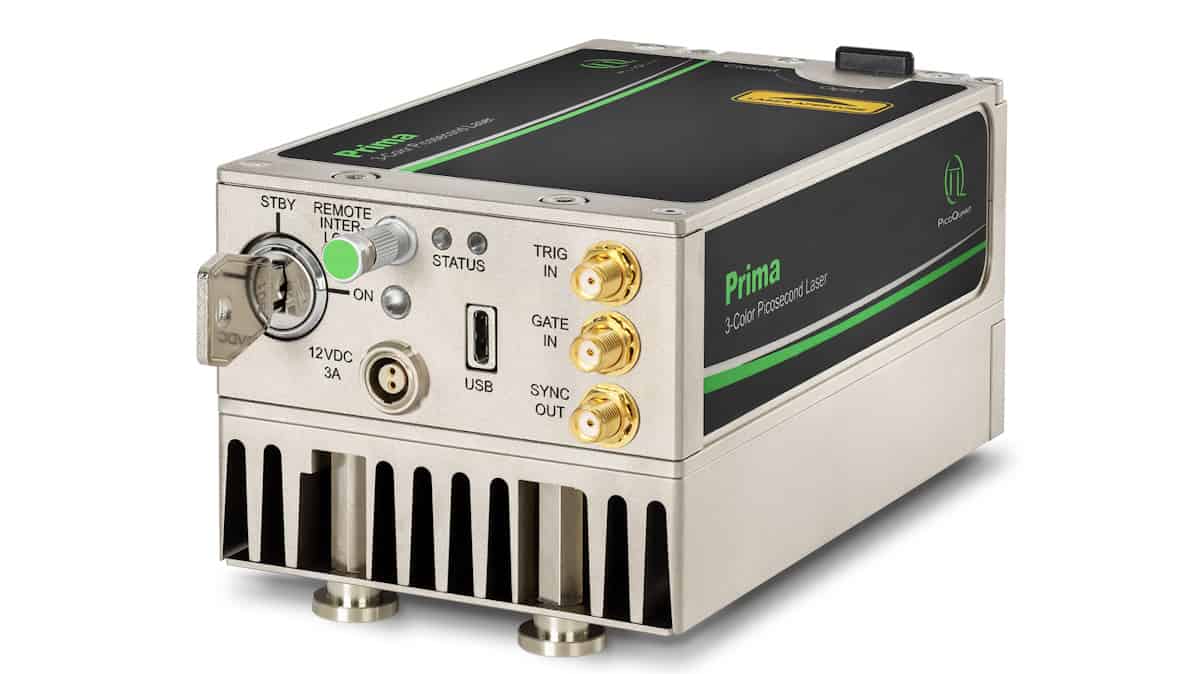
PicoQuant, a specialist in time-resolved spectrometers and microscopes, will be showcasing several recent innovations at LASER World of Photonics. First up is Prima, a compact three-colour picosecond laser module that offers a standalone and affordable solution for researchers who need excitation at 450, 510 and 635 nm within limited lab space. Offering pulsed and continuous-wave operation along with fast switching, Prima is suitable for measuring fluorescence and photoluminescence lifetimes, even in materials that have poor luminescence quantum yield.
Exciting times: the Prima laser module from PicoQuant generates single-frequency light at red, green and blue wavelengths, in either continuous-wave or pulsed-picosecond modes. (Courtesy: PicoQuant)
Also new is the PDA-23 single-photon detector array, developed in collaboration with Pi Imaging, that measures single photons over a spectral range from 400 to 850 nm and beyond. The PDA-23 combines an array of 23 single-photon avalanche detectors, which have a high native fill factor, with microlenses for high photon detection. The low dark count rates, typically around 100 cps, are further reduced with an integrated Peltier-cooler.
The PDA-23 can be combined with the MultiHarp 160, a scalable plug-and-play unit for event timing and time-correlated single-photon counting. This multichannel module supports up to 64 timing channels with high sustained count rates, an ultrashort dead time of less than 650 ps, and a time resolution of 5 ps.
Last but not least is the FluoMic microscope add-on, which can be integrated with the company’s range of FluoTime spectrometers to support time-resolved micro-photoluminescence spectroscopy. Coupling the two instruments together enables both steady-state and time-resolved emission spectra to be captured at high resolution from specific areas of the sample, yielding multi-dimensional datasets that can provide valuable insights for materials science applications.
Visit PicoQuant at booth 216 in Hall B2 to discuss your needs.
Laser simulation software now offers support for GRIN lenses
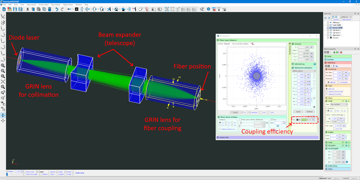
German start-up company BeamXpert has updated its 3D laser simulation software to support GRIN lenses, both for its proprietary, real-time “beam” modelling technique and for the classical ray-tracing approach. The intuitive and easy-to-use software, called BeamXpertDESIGNER, provides an accessible solution for the accurate design of optical systems for laser radiation, delivering ISO-compliant results and available with a perpetual license at an attractive price.
Added functionality: BeamXpertDESIGNER now includes support for GRIN lenses, in this case for coupling the radiation from a diode laser into a single-mode fibre to reduce the sensitivity to misalignment. (Courtesy: BeamXpert GmbH)
The latest version of the software offers other improvements to simplify and streamline the design process. It now includes a comprehensive output of error messages and warnings that indicate possible sources of error, such as intersecting objects or invalid refractive indices, to aid troubleshooting and avoid potential problems. In this context, the ray-tracing engine for the detailed analysis of the aberrations of the simulated optical system has been completely updated. The user interface has also been streamlined, while the software now offers additional options for data export.
Last but not least, the component database has been expanded to include lenses from Thorlabs and GRINTECH. It now consists of more than 20,000 optical components from eleven manufacturers, which can be dragged and dropped directly into the laser simulation set-up.
Find out more about these latest enhancements by visiting BeamXpert at booth 421 in Hall A2. More information can also be found at beamxpert.com.
High-power laser targets demanding applications
HÜBNER Photonics, a manufacturer of high-performance lasers for applications in imaging, detection and analysis, has added a higher power model of its Cobolt Jive 561 nm laser to its 05-01 Series of diode-pumped lasers. Now with a continuous-wave output power of up to 1000 mW, the Cobolt Jive is perfectly suited to demanding applications in fluorescence microscopy, particularly super-resolution techniques like DNA–PAINT, as well as interferometric methods such as particle-flow analysis.
Reliable by design: the Cobolt Jive diode-pumped laser from HÜBNER Photonics delivers continuous-wave power of up to 1000 mW. (Courtesy: HÜBNER Photonics)
The Cobolt Jive is a single-frequency laser that delivers a near-perfect TEM00 (Gaussian) beam with an M2 value of less than 1.1. A proprietary laser-cavity design ensures ultralow noise performance – typically less than 0.1% rms over frequencies from 20 Hz to 20 MHz – as well as an excellent power stability of less than 2% under normal operating conditions.
All Cobolt lasers are manufactured using proprietary HTCure technology, providing a compact package that is hermetically sealed to maximize reliability and provide a high level of immunity to varying environmental conditions. HTCure has proven to be one of the most reliable methods for making industrial-grade lasers, with lasers built using this technology shown to withstand extreme mechanical shocks without any degradation in performance.
Visit HÜBNER Photonics at booth 214 in Hall B2 to explore the company’s full range of high-performance lasers.
The US has released its first strategic framework for space diplomacy. The 37-page document, issued by the US Department of State, outlines the intention to “build international partnerships for civil and national security space”. It calls for the creation of a “rules-based international order” for outer space as well as for the US government to protect the country from “space-enabled threats”.
The document points out that the US private sector is revolutionizing the use of outer space with new technologies and business models. “The number of space-faring nations has dramatically increased,” the document notes. “Countries without current launch capacities are investing in space-based assets and infrastructure.”
A recent estimate suggests that the global space economy was worth $469bn in 2021. As a result of the growth, the framework calls for the responsible stewardship of outer space and to “maximize the benefits of the growing space economy for current and future generations”.
The framework advocates actions across “three pillars”. One involves advancing US space policy and programmes internationally while reducing the potential for conflict. The second is to use US space activities for wider diplomatic goals such as climate change, while the third is to give the state department’s employees the skills to “pursue space-related policy objectives”.
The document also calls for the formation of robust multilateral coalitions such as the Artemis Accords – the agreement among NASA and its equivalents in partner countries on principles that guide lunar exploration.
Tom Stroup, president of the Satellite Industry Association, welcomes the report’s “appreciation for the need for both traditional diplomacy as well as engagement with the US and worldwide commercial space stakeholders”.
Meanwhile, NASA has awarded Blue Origin – the space venture of Amazon founder and Washington Post owner Jeff Bezos – a $3.4bn contract for the third 21st-century human landing on the Moon. NASA has scheduled the launch, tagged Artemis V, no earlier than September 2029. Elon Musk’s SpaceX has the contract for the first two lunar landings in this series.
Secondary dose calculations represent a foundational building block for any patient-specific quality-assurance (QA) programme, providing at-scale validation of radiotherapy treatment plans in the radiation oncology clinic. Front-and-centre in the patient QA endeavour – and in daily use at over 2300 cancer treatment centres worldwide – is LAP’s RadCalc QA secondary check software which, for more than two decades, has provided medical physicists and dosimetrists with automated and independent dosimetric verification of their radiotherapy treatment planning systems (TPS).
An early-adopter and RadCalc devotee is Mauro Iori, director of medical physics at the Institute in Advanced Technologies and Models of Care in Oncology (IRCCS), part of the Azienda Unità Sanitaria Locale (AUSL) di Reggio Emilia in northern Italy. “We have been using RadCalc, in its various iterations, to support independent patient QA for more than 20 years – helping us to reduce our direct dosimetry QA measurements along the way,” explains Iori. “Thanks to LAP’s extensive user base, the software provides a stable, robust and uniform QA environment that integrates seamlessly with our TPS. RadCalc is also vendor-agnostic, so users can standardize the second-check QA workflow across different treatment systems and modalities.”
Monte Carlo insights
Operationally, Iori is one of five clinical physicists and three technicians (dosimetrists) within the AUSL-IRCCS radiation oncology programme, overseeing a suite of two Varian TrueBeam machines, an Accuray TomoTherapy system, a high-dose-rate Elekta brachytherapy unit and an orthovoltage X-ray device. “We treat over 1600 patients each year and cover a wide range of disease indications,” notes Iori (who also manages six other medical physicists and four technicians working in the AUSL-IRCCS radiology and nuclear medicine departments). “What’s more,” he adds, “around 65% of our external-beam radiotherapy treatments involve some form of hypofractionation.” Put simply, that means increased dose per fraction to enable significantly improved patient experience and increased patient throughput – all part of an operational drive for enhanced workflow efficiency.
Mauro Iori: “With RadCalc’s Monte Carlo tools we can achieve the highest quality of dosimetric verification.” (Courtesy: AUSL-IRCCS)
Given AUSL-IRCCS’s clinical emphasis on hypofractionation, Iori and colleagues rely heavily on RadCalc’s Monte Carlo software module for automated 3D dose-volume verification. The goal is to maintain confidence in QA process accuracy across harder-to-treat clinical indications and thereby ensure the planning treatment volume is being covered, while guaranteeing plan quality by comparing dose to adjacent critical structures and organs-at-risk (OARs). Equally important, the medical physics team needs to know if something is not right straight away when treating patients with escalated dose per fraction – in the case of a machine error, for example, or incorrect patient set-up. “For this type of check,” notes Iori, “the log-file analysis and in vivo dosimetry modules in RadCalc constitute a complementary and dedicated tool.”
Under the hood, RadCalc’s Monte Carlo module relies on BEAMnrc (a well-established simulation system for external-beam sources in radiotherapy) utilizing proprietary machine modelling acquired by LAP from McGill University in Canada. The software’s 3D functionality is reinforced by RadCalcAIR (Automated Import and Report) to give users a fully automated second-check process with percent difference, dose-volume histogram (DVH), protocol metrics, gamma and many more customizable tools.
Shedding light on complexity
By allowing 3D verification of plan dose distribution, says Iori, the Monte Carlo module comes into its own for more challenging treatment planning scenarios. Examples include advanced head-and-neck cancers and late-stage prostate and rectal disease – indications that often require larger, heavily modulated treatment fields that are problematic in terms of conventional point-dose QA checks.
Another Monte Carlo clinical use-case arises when treating small or complex tumours surrounded by heterogeneities (e.g. in the lung, abdominal cavities as well as adjacent to bone or metal implants). Planning techniques with steep dose gradients, for example, are especially relevant for lung stereotactic treatments, with the tumour targets generally located near the chest wall, heart and normal blood vessels. Here RadCalc’s Monte Carlo module can perform an accurate and realistic dose verification of TPS plans – implementation of the machine models in BEAMnrc, with every physical component included, establishing confidence in such challenging cases.
The QA workflow in this scenario is all about streamlining: the physicist simply exports the treatment plan via their DICOM RT and RadCalc will automatically verify the plan using a Monte Carlo algorithm, generating results in minutes. If the treatment plan doesn’t pass various preset criteria, RadCalc will prompt the user to investigate what’s going on using a suite of dose analysis tools before determining the course of action (in terms of further preclinical QA or adding in vivo dosimetry checks on the treatment machine).
“With RadCalc’s Monte Carlo tools we can achieve the highest quality of dosimetric verification,” claims Iori, “and not only for simple treatment plans but complex planning scenarios as well, or in the case of adaptive radiotherapy treatments. Right now, we use the Monte Carlo calculations for around 30% of our external-beam radiotherapy patients – chiefly for head-and-neck, thorax and pelvis disease indications that exhibit the highest levels of tissue heterogeneity. Over time, we will extend the use of the Monte Carlo module to all treatment plans.”
The clinical end-game? Better targeting accuracy and dose distribution accuracy – and, ultimately, enhanced treatment outcomes for AUSL-IRCCS cancer patients.
Calculation, simulation, validation
The roll-out of the RadCalc 3D Monte Carlo module at AUSL-IRCCS was preceded by a period of preclinical “tuning and validation”, with the optimized software subsequently used to dosimetrically verify complex treatment plans where the measured dose distributions can be inaccurate due to the TPS dose calculation algorithm.
During the commissioning phase, the AUSL-IRCCS medical physics team, working with colleagues from the University of Bologna in Italy, built Monte Carlo models on the back of specific commissioning measurements. To set up the Monte Carlo module, the team loaded a file containing dosimetric data for different beam energies (6X, 6FFF, 10X, 10FFF) into RadCalc and prepopulated it with values obtained directly from phantom measurements (using defined protocols for percentage depth dose and off-axis ratio).
Another key step involved optimization of the Additional Radiation to Light Field Offset (ARLF) tuning parameter, with Monte Carlo simulations performed on a uniform phantom for four different ARLF values (for each considered energy). The goal here was to achieve the best dose-comparison agreements between Monte Carlo simulations and the volumetric patient-specific QA measurements (with phantom dose distributions and calculated results evaluated in terms of 2 mm/2% gamma pass rate).
“Our preclinical study showed good agreement between Radcalc Monte Carlo simulations and dose measurements, enhancing the dosimetric performance of the secondary-check tool used to verify our treatment plans,” explained Iori. “Following validation, RadCalc’s Monte Carlo module now enables us to better estimate the plan doses in lung-cancer patients and to detect possible inaccuracies due to tissue homogeneity, which are not quantifiable using homogeneous phantoms.”
Ultra-relativistic neutrinos blasted into space during gamma-ray bursts are slowed down by the effects of quantum gravity. That is the conclusion of physicists in Italy, Poland and Norway, who have spotted seven neutrinos that arrived on Earth later than expected, compared to their companion gamma rays.
Quantum theory does a fantastic job of describing interactions that involve three out of the four known forces of nature. However, there is no theory today that adequately describes the quantum nature of gravity. While theories of quantum gravity have been proposed, they tend to make predictions that cannot currently be tested by experiment or observation.
One prediction that physicists have a chance of confirming today is that particles moving very near to the speed of light will lose energy because of a quantum gravitational effect. The faster the particle is moving, the more the effect is enhanced. While the effect is extremely small, if the particles are created in an astrophysical event billions of light-years away, the cumulative result would be a delay that could be measured when the particles arrive on Earth.
Late neutrinos
Now, a team led by Giovanni Amelino-Camelia of the University of Naples have looked for this effect in neutrino data collected by the IceCube Neutrino Observatory. Located at the South Pole, the observatory detects neutrinos when they occasionally interact within a cubic kilometre of ice.
The researchers identified seven neutrinos that have high probabilities of coming from gamma-ray bursts. These are highly energetic events that are produced either by the supernovae of the most massive stars, or by colliding neutron stars. Gamma rays from these specific bursts were also detected by NASA’s Fermi Gamma-ray Space Telescope.
Tantalizingly, these neutrinos appear to have arrived at Earth up to three days after the gamma rays were detected, suggesting that something had delayed them. The three-day delay is expected of particles with energies up to 500 TeV. In comparison, neutrinos with higher energies up to 2 PeV would require a 12-day delay window, which is too long to positively identify them with a specific gamma-ray burst.
Amelino-Camelia explains: “The particles get this extra contribution to their speed, which is negative, and it grows in magnitude as their energy grows”.
Location, location
However, not everyone is convinced. Teppei Katori of Kings College London, who was not involved in the work, points out that the seven candidate neutrinos are all of the “cascade-type”. In a cascade event, a neutrino enters the IceCube Observatory and deposits all of its energy into a small, spherical region, making it difficult to determine the direction that the neutrino came from. This is unlike a “track event”, which produces a signal that points back to the neutrino’s point of origin in the cosmos.
“We don’t know where these neutrinos are coming from exactly,” explains Katori.
Indeed, it is not even clear that gamma-ray bursts do produce a significant number of neutrinos. Katori cites earlier work describing a search for neutrinos from gamma-ray bursts that failed to find a correlation between the two. However, he accepts that this search did not take into account any delays caused by quantum-gravity effects.
In 2022 Katori – who is part of the IceCube collaboration – was a science lead on another experiment looking for quantum gravity effects in neutrinos. Specifically, this study looked at how quantum gravity could affect neutrino oscillations.
Neutrinos come in three different “flavours” – electron, muon and tau – and the particles can oscillate from one flavour to another. Although the experiment found no evidence for quantum gravity affecting neutrino oscillations, it was the first experiment to probe these oscillations at a level where quantum gravity should be relevant. As such, the experiment was able to impose constraints on quantum-gravity models that predict variations in the oscillations.
Implications for cosmology
If quantum gravity is indeed slowing down neutrinos, both Amelino-Camelia and Katori agree that the observation would be a major step forward in understanding quantum gravity and its role in the evolution of the universe.
However, Amelino-Camelia points out, “If the effect is only there for neutrinos and other half-integer spin particles, then the implications for cosmology might be minor.”
For Katori, the most significant outcome of confirming a delay is that physicists could use it to calculate the size of the quantum gravity effect. This would allow physicists to evaluate competing models of quantum gravity – and to take the next step and design experiments and observatories to measure the effect more precisely.
“There is still a gap between quantum-gravity-motivated phenomenology models and quantum-gravity theories,” says Katori. “I think filling this gap is challenging [but] finding any quantum-gravity-motivated effect is the first step.”
The search for neutrinos from gamma-ray bursts will benefit from the construction of IceCube-Gen2, which will increase the size of the detector volume to eight cubic kilometres of ice, improving the ability of the observatory to pinpoint the origins of neutrinos.
From its title, you might expect a book called Force to simply explain how forces work. Instead of a purely educational, fact-driven narrative, however, author Henry Petroski – an engineer and popular-science writer – uses a mix of personal essays, musings and biography to convey how scientific concepts govern and influence everyday life. This is not to say that you won’t learn a fair amount of engineering from Force, or that you won’t come away with a better understanding of how, on a fundamental level, “things work”. But you will also be given the tools to recognize how these things are connected, literally and metaphorically.
Humans have always had the ability to recognize patterns, breaking down complex structures into simpler, recognizable components and using this knowledge to satisfy their curiosity
Force begins by showing how humans have always had the ability to recognize patterns, breaking down complex structures into simpler, recognizable components and using this knowledge to satisfy their curiosity and understand the mechanics of things. Rather than just providing a material understanding of forces, the book delves into how people perceive the world around them, and how these feelings frequently affect our world as much as any physical “pushing or pulling” force does.
In the prologue to Force, Petroski observes that “research and development takes place in a grander context than one of hard physical force; it is also subject to the softer forces imposed by ethics, morals and judgement – none of which is easily and unambiguously defined by laws and limits”. He illustrates this by discussing the medical innovations that brought us from the prehistoric era, when humans had only their five senses to help them avoid harm, to the present day, when technologies such as stethoscopes allow doctors to monitor hearts, lungs and stomachs much more thoroughly than simple listening would permit.
He also mentions how the COVID-19 pandemic spurred innovation, despite the distresses we were under. It led, for example, to the mobilization of vaccines in record time, as well as improvements to mask technology. Although not even close to perfect, today’s masks have undergone major upgrades compared to those worn by, say, plague doctors in medieval Europe.
Petroski complements this sentiment by comparing literal examples of pandemic-driven innovation with more subtle advances made simultaneously in society. During a time when mundane affectionate interactions like embracing, shaking hands and even standing next to someone were heavily discouraged to prevent the spread of the virus, people adapted as best they could, replacing higher-risk gestures with fist and elbow bumps, hip checks and toe taps.
For physicists, one of the most enjoyable parts of Force may be Petroski’s discussion of the work of Michael Faraday, who many (including myself) will know primarily for his discoveries in electromagnetism. Faraday was, however, also well practised and gifted in explaining complex concepts to the public in an easy-to-understand way. As such, people came from far and wide to listen to him speak and to marvel at the practical props he regularly used to assist him – including the rubber balloon, which Faraday invented for his experiments on hydrogen gas.
Much of the book continues in this manner: a case study of a known engineer or piece of engineering, an explanation of how something works on an accessible scientific level, and a discussion that illuminates the social and societal changes that accompanied or indeed motivated it. Each chapter is named after either a fundamental force, a more general derivative force or a feeling you’ll recognize.
The author winds up detailing the inverse square law that governs both gravity and the electromagnetic force, all while weaving in stories of his and his children’s childhoods
In the electromagnetism chapter, for example, Petroski explores how telephones produce and relay sounds. After using older, simpler types of phones to describe the fundamentals of how they work, he moves into the more complex technology of the modern age. Eventually, he winds up detailing the inverse square law that governs both gravity and the electromagnetic force that permeates our planet and the wider universe, all while weaving in stories of his and his children’s childhoods.
Other chapters continue in the same vein, happily building up our idea of what forces can be. As well as the more accessible fundamental forces of electromagnetism and gravity (which gets its own chapter), Force covers everyday sensations such as squeezing a football, feeling inertia on mass transit, and even global effects like winds, hurricanes and earthquakes. It is also chock-full of Petroski’s personal experiences, which gives a biographic feel to the work and makes the explanations very clear.
My favourite example of this blend of the personal and the scientific is Petroski’s account of getting roof tiles replaced on his house. From this mundane and perhaps even annoying task, he creates both a compelling explanation of how gravity works and an opportunity to reveal some of the quirks of his personality. Whereas most of us would try to be anywhere else to avoid the noise, Petroski remained in his attic office, recognizing and enjoying the individual rhythms of the roofers as they hammered in the nails.
In the book’s epilogue, Petroski returns to his earlier medical theme and reflects on the epidemic of bubonic plague that struck London in 1665. During this time, Isaac Newton, like many others who could afford it, sheltered from the disease in the countryside. It was there that he made great strides in physics and (at least in the Western view of science history) discovered gravity after being inspired by the fall of an apple. Though the more recent coronavirus pandemic has been horrendous, Petroski reflects that it also offered unexpected opportunities for some lucky people to change their lives, make progress on their work or become more prepared for the future.
Overall, Force is a great book that roots you in reality and gives solid explanations of some of the world’s most complex phenomena. The accompanying biographical feel is another positive too, as Petroski’s personal experiences from his life and from stories he’s read act as a base for the learning within the book. This gives his narrative a uniqueness and flair when it might otherwise have slipped into a very dry style. Experts and non-experts alike can gain something from it, whether it’s finally understanding how it is that speakers can replicate almost any sound, or simply remembering the countless ways forces impact our day-to-day lives.
Atomic sensor: the device is made of spins whose noise is only limited by intrinsic quantum fluctuations. (Courtesy: E Polzik)
Researchers at the University of Copenhagen in Denmark have found a way to boost the sensitivity of a routine sensing technique known as magnetic induction tomography beyond the standard quantum limit. The improved method could find application in bio- and medical sensing.
In magnetic induction tomography, a magnetic field generated by a current-carrying coil produces minute eddy currents in the sample being analysed. These currents, in turn, alter the magnetic field, which is detected using the collective spin (or magnetization) of an atomic magnetometer. The properties of the detected field yield information about the electrical conductivity and magnetic permeability of the sample.
The technique is used in geophysical surveys, to non-destructively test metallic objects, as well as in medical imaging. But its sensitivity is constrained by the so-called quantum limit, or quantum fluctuations (uncertainty) of the sensor’s collective spin.
“Indeed, quantum mechanics and the uncertainty principle dictate that the spin direction cannot be determined with arbitrary precision,” explains Eugene Polzik, who led this new study. “Roughly speaking, in a sensor that contain N atomic spins, the direction of the collective spin cannot be determined with an angular certainty better than 1/√N, and it is this that we call the standard quantum limit (SQL).”
Reducing uncertainty
Polzik and colleagues showed that this uncertainty can be reduced by using an atomic magnetometer containing atoms whose spins are entangled to generate a so-called spin squeezed state. The angular uncertainty of one of the projections of this state is below the SQL. The researchers arranged the magnetic induction tomography protocol such that the useful signal is contained exactly in the projection with the reduced uncertainty. This approach results in a SQL sensitivity that is almost twice that of conventional atomic magnetometers.
“Conventional magnetic induction tomography techniques use a coil to detect the signal,” explains Polzik. “Such coils have intrinsic thermal noise, as well as picked-up environmental noise, which limits sensitivity. We have used an atomic sensor made of spins whose noise is only limited by intrinsic quantum fluctuations. This allowed us to substantially improve the sensitivity compared to conventional approaches.”
The researchers say they now plan to use their method in bio- and medical sensing, and in particular hope to develop it further for imaging internal organs, including the heart and even the brain.
“We also plan to continue working on this quantum-enhanced magnetic induction tomography with the goal of further improving its sensitivity and spatial resolution,” Polzik tells Physics World.
Glacier surfaces in certain parts of the world contain concerning amounts of toxic radioactive materials, a result of weapons testing and nuclear accidents such as the Chernobyl disaster in 1986. Fallout radionuclides accumulate within cryoconite – a granular sediment found in holes on glacier surfaces – and there is a risk of this material entering local ecosystems as glaciers melt due to climate change. Glaciologists and ecologists say this poses urgent questions. What regions are at highest risk? How diluted is the nuclear material entering proglacial zones? What impact might that have on organisms?
But our ability to build such tiny, powerful chips shouldn’t surprise us. After all, the engineer Gordon Moore – who died on 24 March this year, aged 94 – famously predicted back in 1965 that the number of transistors we can squeeze onto an integrated circuit ought to double every year. Writing for the magazine Electronics (38 114), Moore reckoned that by 1975 it should be possible to fit a quarter of a million components on to a single silicon chip with an area of one square inch (6.25 cm2).
Visionary thinker Gordon Moore, who died in March 2023, co-founded the Intel Corporation in 1968 and later served as chief executive and chairman of the board. (Courtesy: Intel Corporation)
Moore’s prediction, which he later said was simply a “wild extrapolation”, held true, although in 1975 he revised his forecast, predicting that chip densities would double every two years, rather than every year. What thereafter became known as “Moore’s law” proved amazingly accurate, as the ability to pack ever more transistors into a tiny space underpinned the almost non-stop growth of the consumer electronics industry. In truth, it was never an established scientific “law” but more a description of how things had developed in the past as well as a roadmap that the semiconductor industry imposed on itself, driving future development.
Seeing into the future
Basic physics says that as transistors get smaller, they can be run faster and require less power. Simple economics, meanwhile, dictates that as you pack more transistors onto a chip, each transistor becomes cheaper to make. “The cost per component,” Moore noted in his 1965 article, “is nearly inversely proportional to the number of components.” A research director at the US firm Fairchild Semiconductor at the time, Moore simply put the two notions together.
Gordon Moore proved to be a visionary who correctly foresaw the breath-taking pace at which semiconductor technology would grow
In doing so, Moore proved to be a visionary who correctly foresaw the breath-taking pace at which semiconductor technology would grow. While the precise details of how we have shrunk transistors have changed over the years, many of Moore’s predictions about the rise of integrated circuits have come to pass. In his original article, he foresaw digital watches, home computers, smartphones (or what he called “personal portable communications equipment”), the ability to send multiple messages down phone lines, as well as automatic controls for cars.
In an interview with IEEE Spectrum on the 50th anniversary of his 1965 article, Moore said he was surprised that his law had survived for so long. “I never would have anticipated anyone remembering it this far down the road,” he said. Its continuation was, for him, a tribute to the creativity of engineers in the semiconductor industry, who have time and again found new ways to shrink devices. “I could never see more than the next couple of [chip] generations, and after that it looked like [we’d] hit some kind of wall. But those walls keep receding.”
Where will it end? The number of transistors that have been crammed onto integrated circuits has grown at a breath-taking rate since Intel’s first 4004 chip in 1971. Moore’s law, a term coined in 1975, says that the number should double every two years. But continuing the trend is getting harder and ever more expensive to sustain. (This graph is adapted from Wikipedia (wikipedia.org/wiki/Transistor_count) by Hannah Ritchie and Max Roser)
However, in the same interview, Moore recognized that there are two basic physical obstacles that will eventually preclude any further miniaturization. As he recalled the cosmologist Stephen Hawking once pointing out on a visit to Silicon Valley, nothing can travel faster than the speed of light, while materials are, ultimately, made of atoms of a finite size. There are, in other words, speed and size limits to chips. “These are fundamentals I don’t see how we [will] ever get around,” Moore warned. “And in the next couple of generations, we’re right up against them.”
So is the end of Moore’s law in sight?
Gordon Moore: a brief history
Born on 3 January 1929 in Pescadero, California, Gordon Earle Moore was a chemist by training, graduating in 1950 from the University of California, Berkeley. He then did a PhD, also in chemistry, at the California Institute of Technology followed by a postdoc at the Applied Physics Laboratory at Johns Hopkins University from 1953 to 1956. That year he left academia to work at the Shockley Semiconductor Laboratory (SSL), which had just been set up by the physicist William Shockley.
It was an exciting time for the nascent semiconductor industry. SSL was one of the first high-tech firms in Silicon Valley to work on semiconductor devices and Shockley himself was awarded the 1956 Nobel Prize for Physics – along with Walter Brattain and John Bardeen – for their discovery of transistors. Moore was part of a group of talented young scientists whom Shockley recruited to develop and produce new semiconductor devices.
Figures of greatness Gordon Moore (right) in 1978 with his fellow Intel co-founder Robert Noyce (centre), who created the first integrated circuit. On the left is Andrew Grove, who served as the company’s third chief executive from 1987 to 1998. (Courtesy: Intel Corporation)
However, Shockley was not an easy boss to work for, with an authoritarian management style. After a demand for him to be replaced was rebuffed, Moore and other colleagues quit in 1957. Later known as the “traitorous eight”, they immediately founded their own company – Fairchild Semiconductor – with Shockley calling their departure a “betrayal”. The firm was named after Sherman Fairchild, an experienced business executive who invested in the company. It was while working as research director at Fairchild in 1965 that Moore made his famous prediction later dubbed “Moore’s law”.
Fairchild Semiconductor soon grew into a leader in the semiconductor industry, being bought by ON Semiconductor for $2.4bn in 2016. Operating as an incubator for new technology, it was directly or indirectly involved in the creation of dozens of corporations, including Intel and AMD. According to an analysis by Endeavor Insight in 2014, a total of 92 publicly listed firms, with a market value of more than $2.1 trillion, were spawned directly or indirectly by Fairchild. Endeavor reckoned that a further 2000 firms could be traced back to Fairchild too.
Perhaps the most famous of all is Intel, which was set up in 1968 by Moore and the physicist Bob Noyce, a fellow co-founder of Fairchild. Originally known by their initials as NM Electronics, it was soon renamed Intel, and Moore went on to hold various senior roles, including chairman and chief executive. Intel, which pioneered new technologies for computer memory, integrated circuits and microprocessor design, had revenues of $63bn in 2022 and employs more than 125,000 staff.
At his death, Moore was reportedly worth $7bn but he was a prolific philanthropist, setting up the Gordon and Betty Moore Foundation in 2000 with a $5bn gift to support educational and environmental projects. The following year he gave Caltech $600m, which was then the biggest gift to a higher-education institution. Moore also received many honours, including the Presidential Medal of Freedom (America’s highest civilian award) from George Bush in 2002.
Smaller, faster, better
At the heart of any computer is the central processing unit or CPU, which consists of individual transistors linked together to form a single integrated circuit that carries out basic arithmetical operations. The world’s first single-chip microprocessor was the four-bit CPU released by Intel in 1971. Known as the Intel 4004, it had 2300 transistors, each about 10 µm in size and sold for $60. But as Moore predicted, the number of transistors on integrated circuits would quickly rise.
By the early 1980s, transistors were down to 1 µm in size and companies were packing up to 100,000 transistors onto a chip. The number of transistors per chip reached a million by the 1990s, 10 million by the early 2000s and 100 million a decade later. The latest CPUs have over 10 billion transistors using what’s known as a “5 nm process”, with Intel managing to pack over 100 million transistors on each square millimetre by 2019. (These days the process name is essentially a marketing term: the 2 nm of TSMC’s chips, for example, doesn’t actually refer to any specific physical feature on the devices.)
Modern integrated circuits are created by taking a substrate of silicon or some other semiconductor, and then gradually building the circuit up layer by layer using various “lithographic” techniques. There is a huge variety of such methods, but all generally involve using either light or chemical reactions. What’s amazing is not just the incredible progress achieved in making chips, but also the sheer levels of cleanliness that are required in today’s semiconductor fabrication plants.
Back in 1971, the Intel 4004 chip was made using a “10 µm process”, which then meant that all transistors on the chips were spaced no more than 10 µm apart. To achieve such small dimensions, Intel pioneered the use of the “optical mask” – essentially a large, transparent glass plate, parts of which were covered with a pattern of light-absorbing chrome. Blue light was shone through the mask, which was held above the surface of the wafer.
Intel’s clever thinking was to coat the wafer with a light-sensitive organic photoresistive layer, which reacts if light lands on it, while areas that are unexposed stay the same. Using a solvent to dissolve away the parts that had been exposed to light, the original pattern on the mask could then be transferred to the silicon, albeit now much smaller (see image). Several masks steps were used to form the devices needed in the integrated circuit.
Light matters Photolithography has been at the heart of our ability to make ever tinier transistors. It involves covering a silicon substrate with a layer known as a photoresist that reacts if exposed to light. When light is shone through a mask covered in a particular pattern, those parts of the photoresist exposed to light will react, while those parts in the dark remain unchanged. After applying a developer, the substrate ends up with the same pattern as the mask, albeit much smaller.
Over the years, increasingly accurate “projection lenses” had to be introduced between the mask and the wafer to make circuits smaller. In the 1980s, for example, “reduction steppers” were developed to make 2 µm chips. These devices transferred the mask patterns in stages to smaller and smaller lengths. Steppers continued to dominate lithographic patterning throughout the 1990s, as minimum feature sizes reached the 250 nm levels.
Ultimately, however, the smallest feature you can print is limited by two factors: the resolving capability of the photoresist and the minimum size of the image that can be projected onto the wafer. That minimum size – also known as the Rayleigh criterion or the “diffraction limit” – is given by 0.61 λ/NA, where λ is the wavelength of light and NA is the numerical aperture of the projection lens. In other words, it’s impossible to project the image of a feature less than roughly half the wavelength of the light being used.
To get to ever-smaller sizes, lithography systems over the years shifted to ever-shorter wavelengths, progressing from blue (436 nm) to ultraviolet (365 nm) and then to deep ultraviolet light (248 nm), with the latest systems using 193 nm light from an argon fluorine excimer laser. Moore’s law has also been sustained by improvements in numerical apertures, which have been pushed from 0.16 in early systems to amazingly high values of up to 0.93. Huge advances in nano-positioning technology to align the various masks to a suitable accuracy have been vital too.
Down to 2 nm
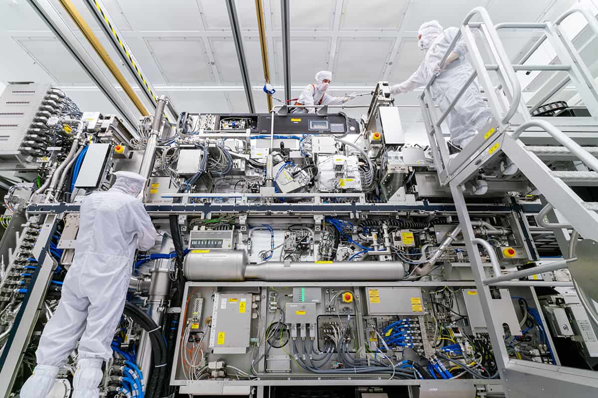
But how do we get to the 2 nm process as used at plants like that of TSMC in Taiwan? That’s well below the diffraction limit even for light with an ultra-short wavelength of 193 nm. Most chip manufacturers have turned to systems developed by the Dutch multinational firm ASML. Using extreme ultraviolet (EUV) light with a wavelength of 13.5 nm, which is almost in the X-ray range, these devices are incredible feats of engineering that push hard on the boundaries of the laws of physics.
The EUV light is created by blasting molten drops of tin with a laser in a vacuum and then bouncing it off mirrors made by Zeiss, which ASML says are the flattest surfaces in the world. Costing more than $150m a pop, each ASML system is huge, having to be shipped to customers in 40 massive freight containers, three cargo planes and more than 20 trucks. Despite the price, the company has so far sold more than 140 of these EUV systems. But as the only supplier, ASML is in fact a bottle neck for expansion of the semiconductor industry.
According to MIT Technology Review, the first generations of chips with tiny EUV features are already being used by Google and Amazon, improving language translation, search-engine results, photo recognition and AI. The EUV revolution is also reaching everyday consumers, with ASML’s machines being used to make chips in smartphones from the likes of Apple and Samsung.
Also helping us to keep Moore’s law going are some amazing advances in materials science and transistor design. Take, for example, “fin field-effect transistors” or FinFETS, which use relatively tall, fin-like structures on the surface of the silicon base. FinFETS were among the first of a new generation of 3D transistors that can be stacked one on top of the other. Companies are already producing devices with 176 mask layers, but 600 layers and above are on the semiconductor industries’ roadmap to deliver future generations of devices.
The latest 2 nm processes use even more advanced FET transistors, known as gate all around (GAA) devices. The US firm IBM has already used them to create chips with a density of 333 million transistors per square millimetre, with the company claiming it can fit 50 billion transistors “onto a chip the size of a fingernail”. IBM says such chips could quadruple smartphone battery life, cut the cost of data centres and make laptops run faster.
Working at the limit
Essentially what is happening is that every possible lever is being pulled to keep Moore’s law on track. ASML, for example, is working towards the 1 nm chip scale using EUV lithography systems, while we can expect to see further improvements in lithography, with the resolution usually halving every six years. It is worth the effort: processors made with TSMC’s 2 nm silicon chips, for example, will run up to 15% faster than with 3 nm devices, while consuming about 25% less energy.
Tiny progress IBM says it can fit 50 billion transistors onto a chip the size of a fingernail using its latest 2nm chip technology. (Courtesy: IBM)
We are certainly not yet done with Moore’s law. Although 2 nm is barely the width of 10 silicon atoms, remember the transistors in 2 nm chips aren’t actually that small; the distance from one gate to another is nearer to 50 nm (the so-called “gate pitch”) so there is a bit more room to play with. We can also wring more out of existing chips by writing software code that is more efficient.
In the end, how far we can stretch Moore’s law is likely to be a matter of pure economics. With TSMC’s newest factory costing $33bn – far more than the $15—20bn of 5 nm plants – sustaining Moore’s law is a game of very high stakes. In this rarefied atmosphere, only a handful of players – IBM, Intel, Samsung and TSMC – are capable of developing next-generation semiconductor chip technology. They certainly haven’t given up on Moore’s law, but further progress is going to be very hard to sustain.
A helping hand A wound-healing ink that can be 3D printed directly into injuries aims to accelerate the body’s natural healing process. (Courtesy: ACS Applied Materials & Interfaces 10.1021/acsami.3c03630)
Repair of chronic wounds, caused by trauma, surgery or diabetes, for example, can be challenging. When the skin is cut or torn, the body works to heal itself, via a complex process involving blood clotting, elimination of any bacterial invaders, regrowth of damaged blood vessels and tissue remodelling.
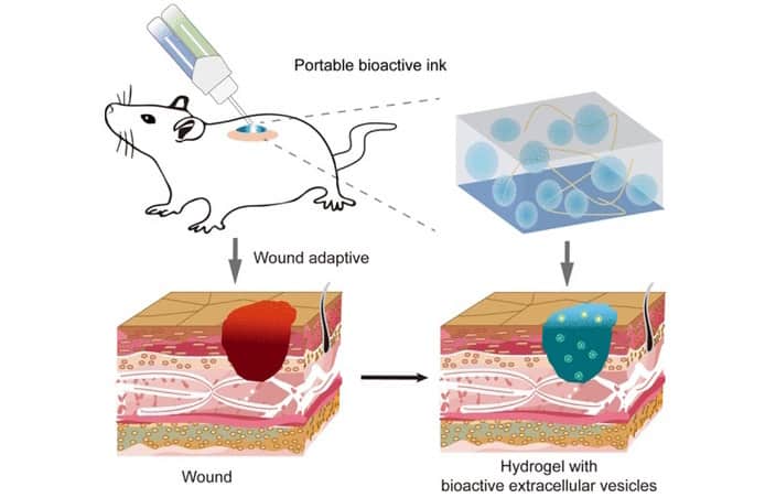
Techniques are available that can help heal wounds, such as applying bandages or stitches to stop bleeding, or using antibiotics to prevent infection. But now, researchers in China have developed a wound-healing ink that aims to actually accelerate the body’s natural healing process, called “portable bioactive ink for tissue healing”, or PAINT. The ink, described in ACS Applied Materials & Interfaces, is made from extracellular vesicles (EVs) embedded in hydrogel and can be painted directly into wounds of any shape using a 3D-printing pen.
EVs secreted from white blood cells such as macrophages play an important role in promoting blood vessel formation and reducing inflammation during healing. To create their PAINT platform, the research team – headed up by Dan Li from Nanjing University, and Xianguang Ding and Lianhui Wang from Nanjing University of Posts and Telecommunications – mixed bioactive EVs derived from M2 macrophages (the type associated with tissue repair) with biocompatible sodium alginate hydrogels. Within minutes, this mixture forms a sturdy EVM2-gel ink that can be applied to wounds in situ.
The researchers first tested the effect of exposing human endothelial cells to various concentrations (0, 100, 200 and 300 µg/ml) of EVM2. In particular, they examined the impact on angiogenesis (the formation of new blood vessels), an essential factor in wound healing.
Cells incubated with EVM2 formed more capillary tubes than untreated controls, with angiogenesis increasing with EVM2 concentration and over time. Optical microscopy showed that the total blood vessel length, vessel percentage area and total number of junctions all increased significantly after 6 h incubation, demonstrating that EVM2 can promote angiogenesis in vitro.
Next, the team incubated macrophages with the three concentrations of EVM2. Macrophages are a vital part of the immune system: they respond to and resist the invasion of foreign substances and play a key role in the repair and regeneration of inured tissues. Polarization of macrophages from the M1 (pro-inflammatory) to the M2 (pro-healing) phenotype is an effective approach for promoting wound healing. Compared with the control group, the ratio of M2 to M1 macrophages significantly increased in the EVM2 groups, indicating that EVM2 promoted polarization to the M2 phenotype in a concentration-dependent manner.
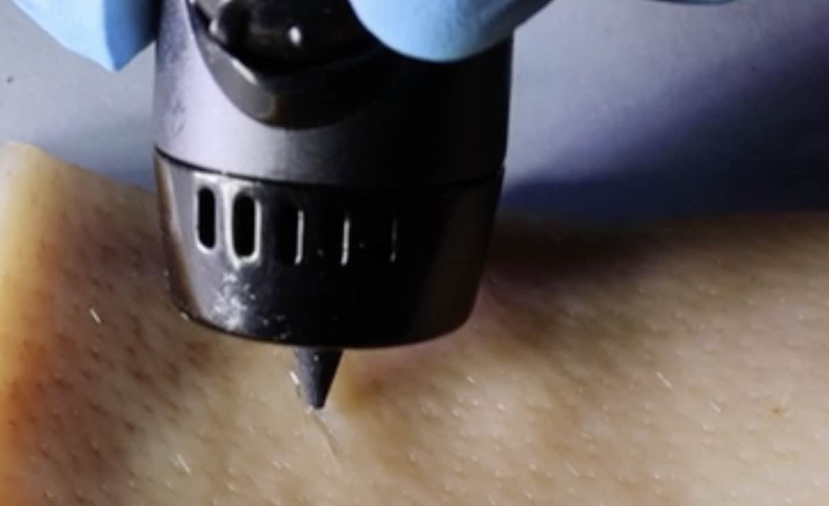
The 3D-printing pen The pen applies a bioactive gel to help wounds heal quickly and effectively. (Courtesy: ACS Applied Materials & Interfaces 10.1021/acsami.3c03630)
Finally, the researchers assessed the therapeutic effect of PAINT in vivo on injured mice. For this, they developed a 3D-printing pen that internally mixes EVM2 with hydrogel precursors to form the EVM2-gel ink at the surface of the skin. This application process can be adapted to match the size and shape of any wound.
Following the creation of a 9 mm circular wound on the back of mice, the animals were treated with EVM2-gel ink containing 100 or 300 µg/ml concentrations of EVM2, or no gel. Fluorescence imaging 6 and 12 h after administration showed that the ink continuously released EVM2 into the wound.
Compared with the control group, mice treated with EVM2-gel experienced significantly accelerated wound healing. On day 12, wound areas were reduced to 21.22, 12.87 and 6.73% of the original size, for the control, 100 and 300 µg/ml groups respectively. Histology indicated that the EVM2-gel ink significantly increased epidermal thickness and promoted collagen fibre formation, essential factors in remodelling newly formed tissues.
Consistent with the in vitro findings, the ink also significantly increased the average microvessel density in the wound area and polarized macrophages to the M2 phenotype. By day 14, scarring gradually decreased and wounds of mice in the 300 µg/ml group were almost completely healed.
The researchers say that this work could help heal a wide variety of cuts quickly and easily, without the need for complex procedures. “Our study demonstrates the high potential of bioactive EV ink in biomedical applications,” they conclude. While the PAINT platform has not yet been tested in human subjects, ultimately, the team plans to work towards clinical translation, Ding tells Physics World.