Machine-learning framework classifies pneumonia on chest X-rays

Pneumonia is a potentially fatal lung infection that progresses rapidly. Patients with pneumonia symptoms – such as a dry, hacking cough, breathing difficulties and high fever – generally receive a stethoscope examination of the lungs, followed by a chest X-ray to confirm diagnosis. Distinguishing between bacterial and viral pneumonia, however, remains a challenge, as both have similar clinical presentation.

Mathematical modelling and artificial intelligence could help improve the accuracy of disease diagnosis from radiographic images. Deep learning has become increasingly popular for medical image classification, and several studies have explored the use of convolutional neural network (CNN) models to automatically identify pneumonia from chest X-ray images. It’s critical, however, to create efficient models that can analyse large numbers of medical images without false negatives.

Now, K M Abubeker and S Baskar at the Karpagam Academy of Higher Education in India have created a novel machine-learning framework for pneumonia classification of chest X-ray images on a graphics processing unit (GPU). They describe their strategy in Machine Learning: Science and Technology.

Training data optimization

The performance of a deep-learning classifier relies on both the neural network model and the quality of the data used to train the network. For medical imaging, the lack of a large enough dataset is a primary cause of subpar performance. To address this shortfall, the researchers used data augmentation, in which new training data are synthesized from existing data (for example via image rotations, shifts and crops) to make the dataset more comprehensive and diverse.

Another method employed to address the lack of appropriate training data is transfer learning – improving a model’s capacity to learn a new task using existing knowledge obtained while performing a related task. In the first phase of their study, Abubeker and Baskar used transfer learning to train nine state-of-the-art neural CNN models to assess whether or not a chest X-ray portrays pneumonia.

For the experiments, they used chest X-ray images from public RSNA Kaggle datasets, including images for training (1341 categorized as normal, 1678 as bacterial pneumonia and 2197 as viral pneumonia), testing (234 normal, 184 bacterial pneumonia, 206 viral pneumonia) and validation (76 normal, 48 bacterial pneumonia, 56 viral pneumonia). Applying geometric augmentation to the dataset expanded it to a total of 2571 normal, 2019 bacterial and 2625 viral pneumonia images.

Based on performance measures including accuracy, recall and the area under the ROC curve (AUROC, a metric summarizing performance over several thresholds), the researchers chose the three top performing CNN models – DenseNet-160, ResNet-121, and VGGNet-16 – for retraining using an ensemble technique.

Ensemble strategy

Rather than relying on a single machine-learning model, ensemble models pool the conclusions of several models to boost performance metrics and minimize errors. The researchers developed a transfer learning-based ensemble strategy called B2-Net and used this with the three selected CNNs to create a final model. They implemented the final B2-Net model on an NVIDIA Jetson Nano GPU computer.
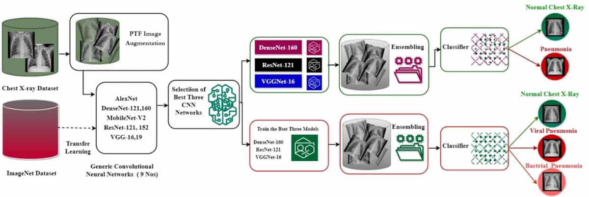
B2-Net model for classifying pneumonia in chest X-rays

They note that during training, some models performed better in identifying normal X-ray images, while others performed better in identifying viral and bacterial pneumonia samples. The ensemble strategy uses a weighted voting technique to provide each classifier with a specific degree of power based on predefined criteria.

The retrained models demonstrated significant improvements in diagnostic accuracy over the baseline models. Testing the models on a balanced dataset revealed that DenseNet-160, ResNet-121 and VGGNet-16 achieved AUROC values of 0.9801, 0.9822 and 0.9955, respectively. The proposed B2-Net ensemble approach, however, outperformed all three, with an AUROC of 0.9977.

The researchers evaluated and validated B2-Net and the other three models using a subset of around 600 chest X-ray images from the pooled dataset. DenseNet-160 misidentified three of the pneumonia test images, while VGGNet-16 and ResNet-121 misdiagnosed one X-ray image each. Overall, the proposed B2-Net approach outperformed all other models, distinguishing between normal cases, bacterial pneumonia and viral pneumonia in chest X-ray images with 97.69% accuracy and a recall rate (the proportion of true positives among the total number of positives) of 100%.

Abubeker and Baskar explain that while the false negative rate is the most critical criterion for a medical image classifier, the proposed B2-Net model provides the best alternative for real-time clinical applications. “This approach, particularly during the present worldwide COVID-19 outbreaks, could assist radiologists in swiftly and reliably diagnosing pneumonia, allowing for early treatment,” they write.

Next, they plan to expand their model to classify more lung disorders, including TB and COVID-19 variants.

Newton’s apple trees for sale, Brazil nut effect without shaking

Do you fancy getting your hands on a descendant of the very tree that inspired Sir Isaac Newton to come up with his theory of gravity? The Times reported this week that the National Trust is working with the UK’s Blue Diamond garden centres to auction 10 saplings that have been propagated from the tree in Woolsthorpe Manor, Lincolnshire.

Newton was born at Woolsthorpe in 1642 and returned there from Cambridge during the plague years of the 1660s. It was then that he apparently came up with his theory of gravity after seeing an apple fall from the tree, which is believed to be 350–400 years old.

The Times says that applications to express an interest in owning one of the saplings can be made next month at the RHS Chelsea Flower Show. The National Trust, which looks after the manor house, will apparently receive at least a quarter of the money raised from the sale. The auction is expected to be held later this year and the money will be allocated to Woolsthorpe and other garden conservation projects.

Brazil nut effect

If you buy your mixed nuts in a can or box you may have noticed that the largest nuts will usually be at the top when you open the container. This phenomenon is called the Brazil nut effect because these nuts are usually the largest in a mixture.

The phenomenon is caused by the shaking of the container during transportation. The standard explanation is that smaller nuts can easily fall between gaps between larger nuts, while the larger nuts cannot fall through gaps between smaller nuts. So the smaller nuts migrate to the bottom of the can, while the larger Brazil nuts rise to the top.

This is an example of granular convection – whereby granular materials flow and separate in response to an external energy source such as shaking. This is an active area of research because the separation of aggregates is relevant to the processing of granular systems ranging from foods to construction materials. This has led to the discovery of a rich set of behaviours, including the reverse Brazil nut effect.

Charged colloidal particles

Now, researchers in the Netherlands and Poland have identified a Brazil nut effect that does not rely on an external source of energy. They looked at electrically-charged plastic particles of different microscopic sizes that were dissolved in an organic solvent. They did not shake this mixture, but rather watched through a microscope as the particles were buffeted about by collisions with solvent molecules – a process called Brownian motion. They found that the larger particles rose to top of the solution, but for very different reasons than in the conventional Brazil nut effect.

In a paper in PNAS, the researchers explain that larger particles in the solution hold more electrical charge, so they feel greater repulsive forces than the smaller particles. This, according to the researchers, allows the larger particles to rise up in the mixture – while the smaller particles cannot do so.

The team believes that the discovery could provide useful insights in fields such as geology and soft matter physics and could also be used to create more stable inks and paints.

Porotech showcases the power of materials science in full colour

Tongtong Zhu, Porotech

So how did Porotech begin?

It all started from a research project in the Cambridge Centre for Gallium Nitride. I was working on single-photon sources for quantum communication, trying to make micro cavities to enhance the coupling between the emitter and the cavity. Probably the easiest micro cavity component is a Bragg mirror, but to make it reflective you need to get a refractive index contrast between different layers.

We could achieve the reflectivity with gallium nitride, but the defects – which you can’t get around – were hindering device performance. So we exploited some of the intrinsic dislocations, which are a common structural defect. Using wet chemistry, we formed a matrix of porous composite between gallium nitride and air. That mixes up the refractive index of the gallium nitride and the air, yielding a much wider parameter for tuning the optical properties.

After doing some business courses, developing a business plan and getting it critiqued, we were confident enough to move out of the university and commercialize our idea

We made the highest-performing single-photon sources in the blue spectrum, but obviously this reflectivity is also beneficial for all kinds of optoelectronics. To make a light-emitting diode (LED), you need the bottom mirror to reflect light and then be able to extract the photon. We tested it – and it worked beautifully. After doing some business courses, developing a business plan and getting it critiqued, we were confident enough to move out of the university and commercialize our idea.

You won a Business Start-up Award from the Institute of Physics in 2022 for making a red indium gallium nitride LED. What was the biggest challenge to that innovation – and how did you overcome it?

Red is not that difficult to achieve with other materials, like gallium phosphide or gallium arsenide. On paper, it should also be achievable with gallium nitride, in terms of the band gaps defined by the material. But defects are a problem – as you go to from blue to green and then even longer wavelengths, you need to put more indium in the light-emitting area, which makes the quantum wells thicker.

And the trouble with gallium nitride compared to many other compound semiconductors is that the lattice parameter mismatch is huge between different alloys. So you get a lot of strain, and if that’s not properly relieved, you will incur lots of defects that will hinder the LED’s performance. If you add more indium atoms, there is also a risk of phase separation, where they will just stay as metal platelets rather than forming crystalline materials.

We then build on top of this beautiful porous architecture so we can manipulate the material’s optical and mechanical properties. We can actually change the mechanical property and enlarge the lattice parameter in a simple way so that it can be more matched to the light-emitting area – the high-indium-content region that we are trying to build on top. The closer match we can get, the fewer problems we will encounter in the light-emitting area.

What are the implications of having a red indium gallium nitride LED alongside green and blue ones?

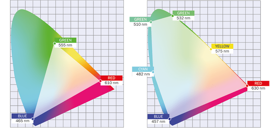
Blue and green are already very successful and established using gallium nitride, but industry currently has had to use other sources like gallium arsenide for the red. That’s really costly, both in terms of capital expenditure and throughput. What’s more, mixing different materials substantially reduces the yield, and subsequently the adoption rate as well. Getting all the colours from a single material means we can use the existing supply chain making blue and green and use them to generate red as well – without any additional capital expenditure or complications with the processing flow.

You’ve also made tunable wavelength emitters, what you call DynamicPixelTuning®. How do they work and alter the picture you just described?

It was an accident in a way. By extending the wavelength capability of gallium nitride to red, we found out we can actually also shift the colour to the other side of the spectrum. Fundamentally, with gallium nitride there is some internal strain, which really affects how the quantum wells and the band gap react when an external bias is applied. Everybody wants to achieve a stable single colour, but when you inject a current, that external bias will affect the internal field, varying the wavebands.

We can reduce the strain, which would improve the stability, but we can’t eliminate 100% of the internal field just by material manipulation. We wondered if we could capitalize on the strain status and enlarge that internal field, so when we apply an external bias, the shift is large enough that we can have all the colours. In fact, we can now achieve the large wavelength shift in a controllable way. It’s a very linear relationship, so you can have any colour as a function of the current density.

So we have two ways of approaching the market and working with existing capabilities, depending on the complexity of a customer’s system and their display requirements.

Porotech-colour-space-diagram

What’s next for Porotech? Are you looking to expand?

For us it’s very important to pull in customers on the one hand, but also to spread our risk. We don’t want to be betting on just one market segment, so we are looking at three major areas: large TV and signage; smart wearables; and AR/VR. With the first area, we’re talking about new high-end TVs with 100-inch displays, that no other existing technology can implement so cost-effectively.

Our technology can enable sense and touch functionality, which will help smart wearables to become more personalized items in future

As for smart wearables, we’re talking smart watches, goggles and glasses. The micro LED fundamentally is a display technology, but it’s building on top of the semiconductor ecosystem and the integration with silicon transistors, so it promises integrability and other functionality as well. It can give display information but can also enable sense and touch functionality, which will help smart wearables to become more personalized items in future.

For AR/VR we are also trying to contribute on top of the micro LED, the photon, the light output and the optoelectronics. We’re also focusing on the future integration with the silicon foundries and silicon transistors. Obviously that’s a lot harder because of the restricted weight and small volume that’s required for the AR/VR to be implemented on simple glasses.

So we are more commercially ready for the big TV and smart watches, but for AR it’s more about the system-level integration and engineering.

You started out as an academic, so it must have been a learning curve for you to learn how to talk about supply chains, capital expenditure and integrating your product with different devices

I’m still learning actually, and I’ve been quite happy taking on that challenge. I could have pursued academic excellence, but since we’re doing applied science and materials, we really have to focus on how to implement that to benefit industry and people. So I felt quite pumped-up initially, that I chose this route to new personal development.

You realize very early on you are less capable, less knowledgeable, and you don’t have any experience. You have to learn from other people. It was very good that the Cambridge ecosystem provides all that mentoring on top of the university support. That’s why we spent a couple of years hopping inside and outside the university, using some of the resources, doing market research and getting ourselves trained up.

Learning is an everlasting process as we continue to grow, but it is a very worthwhile investment.

Do you have any advice for people seeking to turn their technology into a commercial product?

My advice would be to listen more and talk less. Technology is good, physics is wonderful, but that’s only one-third or one-quarter of the problem. You’re going to need people, resources and a strategy for how to transfer the technology into a real product and get the business plan to support it. You’ll need to engage with a wider community to hear different views and critiques. Take that feedback and reflect on it to improve yourself and your ideas.

I think that’s a hard learning curve that everybody has to go through. But admitting that you are not capable of everything from the beginning, and learning from more experienced people is very important. One small company can’t do everything by itself. You need a lot of help from university, government, supply chain and customers and partners, even your family and friends. So listen more and reflect on a personal level. That’s what I would recommend.

Lithium-ion batteries break energy density record

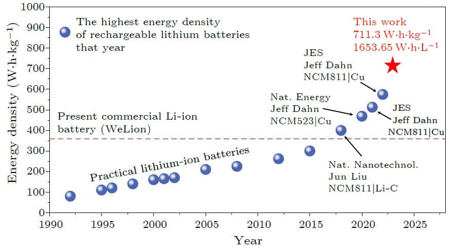
Graphic showing that the energy density of lithium-ion batteries has increased from 80 Wh/kg to around 300 Wh/kg since the beginning of the 1990s

Researchers have succeeded in making rechargeable pouch-type lithium batteries with a record-breaking energy density of over 700 Wh/kg. The new design comprises a high-capacity lithium-rich manganese-based cathode and a thin lithium metal anode with high specific energy. If developed further, the device could find use in applications such as electric aviation, which requires much higher energy density batteries than those available today.

Lithium-ion batteries are a key technology for helping to reach climate neutrality goals. They are increasingly being used to power electric vehicles and as the principal components of domestic devices that store energy generated from renewable sources. The technology has greatly advanced too: since first commercialized by Sony in 1991, the energy density of lithium-ion batteries has increased from 80 Wh/kg to around 300 Wh/kg.

Achieving a truly carbon-free economy, however, will require better-performing batteries than current lithium-ion technology can deliver. In electric vehicles, for example, a key consideration is for batteries to be as small and lightweight as possible. Achieving that goal calls for energy densities that are higher than 400 Wh/kg. The problem is that today’s lithium-ion batteries mainly contain intercalation-type cathodes (for example, LiFePO4, LiCoO2 or LiNixMnyCozO2, x+y+z=1) and graphite-based anodes, and the energy density of these electrodes is approaching its upper limit.

High charge-discharge voltage

In the new work, the researchers led by Xiqian Yu and Hong Li of the Institute of Physics, Chinese Academy of Sciences in Beijing, have manufactured practical pouch-type rechargeable lithium batteries by using an ultrathick high-discharge capacity Li1.2Ni0.13Co0.13Mn0.54O2 cathode with an areal capacity exceeding 10 mAh/cm2 and a lithium metal anode. The high charge-discharge voltage of the lithium-rich manganese-based oxides allows for a higher lithium-ion storage capacity.

“The anode electrode employs ultrathin metal lithium incorporated using a separator coating technique, which addresses the annoying issue of reversible deposition of ultrathin lithium of large surface capacity,” explains first author Quan Li.

The devices boast a gravimetric energy density of 711.3 Wh/kg and a volumetric energy density of 1653.65 Wh/L, both of which are the highest in rechargeable lithium batteries based on an intercalation-type cathode, Li tells Physics World.

“With respect to the battery manufacture, our extremity battery structure design (including the use of ultrathin current collectors) was tailored to minimize the usage of auxiliary materials while enhancing the proportion of active materials in the entire battery,” he adds. “This synergistic approach is what enabled the ultrahigh energy density of the batteries.”

Long-range electric vehicles and electric aviation could benefit

The new devices could benefit long-range electric vehicles and electric aviation, both of which place increasingly high demands on battery energy density. The research could also help address some of the inherent issues associated with battery technology, says Li.

“For instance, it offers insights into how to balance safety and other important factors in high-energy density batteries, which will help in the practical realization of high-energy density batteries in the future. Research on batteries with energy densities approaching theoretical limits will also help improve our knowledge of solid-state ionics and solid-state electrochemistry, allowing perhaps for technological innovation in new materials and battery systems.”

The researchers, who report their work in Chinese Physics Letters, explain that a trade-off always exists between the energy density, cycle performance, rate capability and safety of lithium-ion batteries. Safety is a primary requirement, but elevated energy density will increase the risks during battery operation, they say. “Energy density must be gradually improved while ensuring safety,” says Li. “Our goal is to enhance battery safety performance through solid-state battery technology, making high-energy density batteries more practical.”

The cycle performance of high-energy density batteries also still lags behind that of currently commercialized batteries, he adds. “This parameter needs to be comprehensively considered to meet the requirements of specific fields. It will therefore take considerable time for ultrahigh-energy density batteries to be practically applied. Addressing the challenges that hinder their practical usage will be the ongoing direction of our future research endeavours.”

Giant magnetoresistance spotted in near-pristine graphene

After amazing us with its incredible strength, flexibility and thermal conductivity, graphene has now chalked up another remarkable property with its magnetoresistance. Researchers in the UK have shown that, in near-pristine monolayer graphene, the room-temperature magnetoresistance can be orders of magnitude higher than in any other material. It could therefore provide both a platform for exploring exotic physics and potentially a tool for improving electronic devices.

Magnetoresistance is a change in electrical resistance on exposure to a magnetic field. In the classical regime, magnetoresistance arises because the magnetic field curves the trajectories of flowing charges by the Lorentz force.  In traditional metals, in which conduction occurs almost solely through electron motion, magnetoresistance quickly saturates as the field increases because the deflection of the electrons creates a net potential difference across the material, which counteracts the Lorentz potential. The situation is different in semimetals such as bismuth and graphite, in which current is carried equally by electrons and positive holes. Opposite charges flowing in opposite directions end up being deflected the same way by the magnetic field, so no net potential difference is generated and the magnetoresistance can theoretically grow indefinitely.

In this regime, the magnetoresistance depends on the mobility of the charge carriers (their propensity to move in response to an applied potential). Counterintuitively, therefore, materials with higher carrier mobility also show higher magnetoresistance. The magnetoresistance of most semimetals drops as temperature rises because thermal vibration leads to scattering. Experiments on magnetoresistance are usually conducted, therefore, under cryogenic conditions.

No bandgap

Graphene, however, is known for its extraordinarily high carrier mobility, which arises because electrons propagate as massless Dirac fermions at about 10m/s regardless of their energy, and for its complete absence of any bandgap. Now, the University of Manchester’s Andre Geim and Alexey Berdyugin and Leonid Ponomarenko at the University of Lancaster colleagues have looked at whether colossal magnetoresistance could be created in graphene by filling up the electronic energy levels precisely to the point where the valence and conduction bands touched.

“We tune the Fermi level to this singularity spot and, if you have a non-zero temperature, then at equilibrium you will have a certain number of electrons excited from the valence band to the conduction band, leaving behind an equal number of positive holes in the valence band,” explains Berdyugin.

The electrical properties of graphene were first measured nearly 20 years ago by Geim and Kostya Novoselov at the University of Manchester – bagging the duo the 2010 Nobel Prize for Physics. However, Berdyugin explains that experiments involving pristine undoped graphene are very difficult to do. “You never actually get to the so-called charge neutrality point. You have an island of doping with electrons in one place, an island of doping with holes in another – on average you have the neutrality point but in fact it consists of doped graphene. Such situations are referred to as electron-hole puddles.” In the subsequent two decades, the homogeneity of graphene has improved by orders of magnitude and the size of the electron–hole puddles has consequently reduced, but it is still present.

Dirac fluid

When the temperature is raised, however, the small inhomogeities in the doping can be overwhelmed by thermal fluctuations, producing a “Dirac fluid” with unexpected properties such as hydrodynamic flow. In the new work, the Manchester and Lancaster researchers show that, in this state, this Dirac fluid exhibits a room-temperature magnetoresistivity of 110% in a magnetic field of 0.1 T. In contrast, metals rarely show magnetoresistivities more than 1% above liquid nitrogen temperature at the same magnetic field. Graphene’s high magnetoresistance could potentially be useful for magnetic sensing.

More interesting from a theoretical perspective is the behaviour of the Dirac fluid in high fields. Whereas the classical model of magnetoresistivity predicts a parabolic increase of resistance with field strength, in graphene it begins to increase linearly. Similar phenomena have been observed in strongly interacting systems such as high-temperature superconductors, and an explanation was proposed by the Nobel laureate Alexei Abrikosov. So far, however, this curious effect is not properly understood in 3D, and whether it would be observed in graphene was unknown. “Theory can predict almost anything,” says Berdyugin, “but to make predictions theoreticians have to make assumptions, and sometimes when they face reality they don’t hold. Here we show theory the correct way to look at the charge neutrality point of graphene.”

Condensed-matter physicist Mark Ku of the University of Delaware is intrigued by the research. “By itself, I wouldn’t say the large magnetoresistance is the most interesting or novel part,” he says. “I’m not sure I would say it’s surprising because I’m not sure what people actually expected, but what is certainly clear is that there is no current theory to explain their observed magnetoresistance in the Dirac fluid…I think that’s the most novel part because people know that if they have a theory, they can compare it to the experiment.”

The research is described in Nature.  

The ORCA-Quest camera with qCMOS technology from Hamamatsu

In this short video filmed at the American Physical Society March Meeting in Las Vegas, Brad Coyle, OEM camera product manager at Hamamatsu, introduces its ORCA-Quest camera with qCMOS engineering.

This new technology provides quantitative CMOS data collection – in other words, it can record the number of photons that impact on each individual pixel. The ORCA-Quest camera enables the system to upload a lot of data at high speed and improve data quality – both for high speed and high fidelity information.

This feature could be vital for quantum computing and quantum communication. It is also suitable for live imaging, for example, to look at events dynamically in cells or getting real-time feedback from the camera. Hamamatsu is looking to hear from partners who may have a unique application for this camera and the new technology it brings.

Quantum technologies promise a secure future for cryptography

This episode of the Physics World Weekly podcast features an interview with Chris Schnabel, who talks about the threats and opportunities that quantum technologies pose to organizations that rely on cryptographic systems.

Schnabel is vice president of product at Qrypt, a US-based company that uses quantum technology to generate random numbers for cryptography and other applications. He explains how modern cryptography systems could be compromised by quantum computers of the future – and how quantum technologies can be used to achieve secure communications.

Giant orbital magnetic moment appears in a graphene quantum dot

A giant orbital magnetic moment exists in graphene quantum dots, according to new work by physicists at the University of California Santa Cruz in the US. As well as being of fundamental interest for studying systems with relativistic electrons – that is those travelling at near-light speeds – the work could be important for quantum information science since these moments could encode information.

Graphene, a sheet of carbon just one atom thick, has a number of unique electronic properties, many of which arise from the fact that it is a semiconductor with a zero-energy gap between its valence and conduction bands. Near where the two bands meet, the relationship between the energy and momentum of charge carriers (electrons and holes) in the material is described by the Dirac equation and resembles that of a photon, which is massless.

These bands, called Dirac cones, enable the charge carriers to travel through graphene at extremely high, “ultra-relativistic” speeds approaching that of light. This extremely high mobility means that graphene-based electronic devices such as transistors could be faster than any that exist today.

When these electrons are confined in a graphene quantum dot, which is a nanoscale structure, they travel at high speeds in circular loops around the edge of these dots, thereby creating orbital magnetic moments. These moments have energies of up to around 70 meV/T and a value of around 600 Bohr magnetons (µB, a physical constant that expresses the magnetic moment of an electron created by its orbital or spin angular momentum).

Giant magnetic moments

In the new work, a team led by Jairo Velasco Jr built on a technique that Velasco and his previous colleagues pioneered in 2015. The researchers produced quantum dots with extremely sharp confinement potentials that trapped graphene electrons travelling near the edge of the nanoscale structure. They then measured the way that the states of these electrons responded to an externally applied magnetic field.

“This allowed us to discover that the states possess giant magnetic moments, a property that endows them with an acute sensitivity to magnetic fields,” says Velasco. “Our theory collaborators Sergey Slizovskiy and Vladimir Fal’ko pointed out that the giant magnetic moments of these states stem from their extreme speeds (near the speed of light).”

The moments’ sensitivity to external fields could allow them to be used as quantum sensors that can detect and therefore map these fields at the nanoscale with high resolution, say the researchers.

“The fast electronic states that live at the edge of the graphene quantum dot can also be thought of as a persistent current – that is, one that does not require an external source to circulate,” Velasco tells Physics World. “Such systems have been studied previously in metallic rings and are of fundamental interest. The currents studied in our experiment could potentially be useful for encoding information or simulating quantum systems.”

In their present work, which they detail in Nature Nanotechnology, the UC Santa Cruz researchers also showed that two quantum dots coupled together have orbital magnetic moments that are different again. In the future, they say they would like to make more complicated coupled structures such as chains or a so-called frustrated system like triangles. “These more complex systems could host new quantum ground states based on our newly discovered relativistic orbital magnetic moments.”

 ‘Negative temperature’ thermodynamics is observed in a photon gas

Researchers in Germany and the US have created photon gases that can exist at “negative temperatures” while undergoing basic thermodynamic processes – including expansion and compression. The research could lead to the development of new optical technologies including those for data transmission.

When a gas is cooled to very low temperatures, its particles will occupy the lowest available energy states in the system. As the gas becomes warmer, some particles will occupy higher energy states. This occupation can be done in a number of different ways and this diversity is characterized in terms of an increasing entropy.

Normally, there is no limit on the number of energy states that the particles can access and the entropy of a system can go on increasing as the system gets hotter. However, if there is a limit on the number of energy states, then the entropy will not increase as more energy is put into the system. Indeed, the entropy will decrease because the particles will become packed into the highest energy states. Such a system is similar to a low temperature system in which all the particles are packed into the lowest energy states.

Decreasing entropy

In 1949 Lars Onsager introduced the concept of “negative temperature” to describe the thermodynamic relationship between entropy and energy in such a system. As the negative temperature increases to zero from below, the energy of the system increases and the entropy decreases.

“Negative temperatures have been experimentally demonstrated in platforms such as spin systems, cold atom lattices, and most recently, vortex clusters in 2D quantum systems,” explains Demetri Christodoulides at the University of Central Florida. “However, realizing basic thermodynamic processes in the negative temperature regime has not yet been achieved.”

In a new study, Christodoulides along with Ulf Peschel at Friedrich Schiller University Jena and colleagues, explored a new experimental approach to negative temperatures. This involved exploiting nonlinear interactions between ensembles of photons travelling through thin optical fibres.

Coupled fibre loops

Their experiment involved firing pulses of light through two coupled fibre loops with slightly different lengths. This caused the photons in these ensembles to travel with distributions of velocities defined by temperature – just like the particles in a regular gas. However, the possibilities presented by the experiment stretched beyond the limitations of more conventional thermodynamic systems.

“By nature, these classical photonic configurations are governed by their own laws,” Christodoulides explains. “As such, nonlinear photonic systems can serve as a versatile platform upon which one can now observe a host of previously unknown phenomena, that would have been otherwise inaccessible in other thermodynamic settings.”

Crucially, Peschel and Christodoulides’ team could create a scenario that would have been impossible in a regular gas: a system in which all velocity states available to the photons were equally likely to be occupied. At this stage, the photons had reached their maximum possible entropy, creating a gas with an infinite temperature.

When the researchers added more energy to the coupled loops, the distribution of photon velocities began to decrease, as the photons moved towards a single, maximum velocity state.

Basic thermodynamic processes

For the first time, this enabled the team to observe basic thermodynamic processes that have so far eluded physicists studying more exotic systems in negative temperature regimes. “We observed all-optical isentropic expansions and compressions, as well as irreversible Joule expansion effects, through stable negative temperature distributions,” Christodoulides explains.

In future research, the team hopes to create negative temperature regimes in other degrees of freedom available to photons beyond their velocity: including space, frequency, and polarization. Ultimately, this could enable researchers to fine-tune the properties of light in fascinating new ways – possibly leading to more robust and reliable optical signals, which are better suited to large-scale data transmission.

Christodoulides adds, “Our approach could also provide a route for manipulating Bose-Einstein condensates and optomechanical systems as well as for developing high-brightness optical sources based on light cooling schemes.”

The research is described in Science.

Laser-printed electronics could create next-generation medical implants

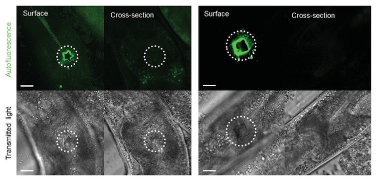
3D printing onto an anesthetized worm's head

Researchers at Lancaster University have succeeded in directly printing three-dimensional conducting polymer structures inside a living organism. While the process is in its very early stages, if properly developed, it could be used to print next-generation implants for a variety of medical applications, including real-time health monitoring and interventions such as neuromodulation. Human–computer interfaces might also be a possibility.

The researchers, co-led by materials chemist John Hardy, used a high-resolution fast pulsed laser 3D printer to generate volume pixels (voxels) in which two photons of light with a wavelength of roughly 780 nm excite a molecule (in this case the photoinitiator Irgacure 2959) from one energy state to a higher energy state in a single quantum event. This in turn initiates polymerization of the constituent monomers in the printer “ink”. The polymerized product, polypyrrole, is electrically conductive and can thus be used to build electronic circuits.

“We started with proof-of-concept studies to print an electrical circuit within an elastomer (polydimethylsiloxane, PDMS) matrix and used the electrical contact points printed on top of the PDMS to stimulate neurones in a slice of mouse brain tissue that were kept alive in vitro, evoking neuronal responses that were similar to those seen in vivo by our colleague Damian Cummings at University College London,” explains Hardy.

The researchers adapted this additive manufacturing process to work directly in nematode worms (C. elegans). “While printing in live worms sounds simple in theory, it was not a given,” explains co-team leader Alexandre Benedetto. “We needed to make sure that the precursor monomer mixture was biocompatible, which is more difficult than once the material is polymerized and ‘inert’, and that the light used to polymerize the monomer does not harm the animals by burning surrounding tissue. This was possible because we used lower energy lasers and a ‘two-photon’ set-up.”

The researchers also had to immobilize the worms during the 3D printing procedure to stop them from wiggling, he adds. “To do this, we anaesthetized them and trapped them between two glass coverslips containing micro-channels made of transparent silicon. These grooves were moulded on a piece of old vinyl record disc.

The roundworms ingested some of the ink and, because they are transparent, it was possible to focus the laser beam within them. Their transparency also makes them more vulnerable to heat, light and desiccation than human skin – so printing on these animals therefore represents a significant step towards de-risking the technology.

The researchers, who report their work in Advanced Materials Technologies, hope to print more complex circuits in the future using their technique. They are now looking into the scope of the structures that they can print inside and on live biological tissue. The ethical implications of the research also need to be addressed. They say they will be doing this part of their project with colleague John Appleby.

“If we think about applying this type of approach to human health, the 3D printing set-up needs to be modified since we will not be dealing with microscopic or very thin objects,” Benedetto tells Physics World. “One way to do this is to miniaturize the 3D printing equipment so that it can be hand- or robotic-arm-held.”

Copyright © 2026 by IOP Publishing Ltd and individual contributors