This episode of the Physics World Weekly podcast features an interview with Sumner Norman, who is chief neuroscientist at the US-based company AE Studio. The firm is creating an operating system for brain–computer interfaces (BCIs) and Norman explains how BCIs could benefit people with neurological disorders and injuries.
A new technique makes it possible to capture videos of single atoms “swimming” at the interface between a solid and a liquid for the first time. The approach uses stacks of two-dimensional materials to trap the liquid, making it compatible with characterization techniques that usually require vacuum conditions. It could enable researchers to better understand how atoms behave at these interfaces, which play a crucial role in devices such as batteries, catalytic systems and separation membranes.
Several techniques exist to image single atoms, including scanning tunnelling microscopy (STM) and transmission electron microscopy (TEM). However, they involve exposing atoms on the surface of the sample to a high-vacuum environment, which can change the material’s structure. Techniques that do not require a vacuum, meanwhile, are either lower-resolution or only work for short time periods, meaning that the atoms’ motion cannot be captured on video.
Researchers led by materials scientists Sarah Haigh of the University of Manchester’s National Graphene Institute (NGI) have now developed a new approach that enables them to track the motion of single atoms on a surface when that surface is surrounded by liquid. They showed that the atoms behave very differently under these circumstances than they do in vacuum. “This is crucial,” explains Haigh, “since we want to understand atomic behaviour for realistic reaction/environmental conditions that the material will experience in use – for example, in a battery, supercapacitor and membrane reaction vessels.”
Sample suspended between two thin layers of liquid
In their experiments, the NGI researchers sandwiched their sample – in this case, atomically-thin sheets of molybdenum disulphide – between two sheets of boron nitride (BN) in a TEM. They then used lithography to etch holes in specific regions of the BN so that the sample could be suspended in the areas where the holes overlapped. Finally, they added two graphene layers above and below the BN and used these to trap a liquid in the holes. The resulting structure, in which the sample is suspended between two layers of liquid, is just 70 nm thick, Haigh tells Physics World.
Thanks to this so-called double graphene liquid cell, the researchers were able to acquire videos of the single atoms “swimming” while surrounded by liquid. By then analysing how the atoms moved in the videos and comparing this motion to theoretical models developed by colleagues at the University of Cambridge, they obtained fresh insights into how a liquid environment affects atomic behaviour. For example, they found that the liquid accelerates the atoms’ movement while also changing their preferred “resting sites” with respect to the underlying solid.
“The new technique could help improve our understanding of the behaviour of atoms at solid-liquid interfaces,” Haigh says. “Such interfacial behaviour is generally only probed at lower resolution, but it determines the lifetime of batteries, the activity and longevity of many catalytic systems, the functionality of separation membranes as well as many other applications.”
The researchers say they are now studying a wider range of materials and how their behaviour changes for different liquid environments. “The aim here is to optimize the synthesis of improved materials that will be needed for the net zero energy transition,” Haigh concludes.
Researchers in the UK have done calculations that show how “twisted light” can be used to manipulate the ultracold atoms in an exotic state of matter called a Bose–Einstein condensate (BEC). Using theoretical models, Grant Henderson and colleagues at the UK’s University of Strathclyde discovered that light–matter solitons could be generated through the interaction between corkscrew-shaped wavefronts of light and BECs.
BECs are an exotic state of matter, in which a gas of identical atoms is cooled close to absolute zero. This drives a large fraction of the atoms into the lowest quantum state, and when this occurs the physics of the gas is defined by a macroscopic wave function.
One particularly interesting feature of BECs are solitons, which are wave packets that maintain their shapes as they travel. Solitons are also found across a wide array of fields, including hydrodynamics, ferroelectric materials and superconductors.
A spatial optical soliton occurs when the diffraction of light in a medium is carefully balanced by self-focusing. Self-focusing is a non-linear effect that involves the light itself changing the optical properties of the medium.
Twisting dipoles
In their study, Henderson’s team explored a more complex scenario. Instead of a conventional laser beam with a Gaussian intensity distribution, they considered “twisted” light. This is light with a wavefront that twists around its axis of travel like a corkscrew. These beams carry orbital angular momentum, which means that they can rotate atomic-scale electric dipoles that they encounter in a medium.
The team calculated what would happen when a beam of twisted light interacts with the atoms of a BEC that is moving in the same direction as the light. They predict that the self-focusing effect would cause the the twisted light to fragment into solitons. Since the BEC’s atoms are attracted to high-intensity light, the atoms would be “captured” by the optical solitons. The result is the creation of coupled light–atom wave packets.
The atoms in these packets twist as they propagate, and the team found that the number of packets created is equal to twice the orbital angular momentum of the twisted light. The above figure, for example shows the creation of the four solitons that would occur when light with an orbital angular momentum of two interacts with a BEC.
The discovery presents a simple new technique for sculpting exotic matter into complex shapes, and carefully controlling the transport of BEC atoms. Henderson and colleagues now propose that the effect could be harnessed in novel quantum technologies: including ultra-sensitive detectors, and circuits that use neutral atoms to convey currents.
Lighting up the world Photonics has countless applications, including energy-efficient, pesticide-free “vertical farming”. (Courtesy: iStock/Supersmario)
Which industry employs twice as many people in the UK as pharmaceuticals and more than either the space or “fintech” sectors? The answer is photonics, according to the Photonics Leadership Group (PLG) – a trade association representing more than 120 members in the field. For the last few years, it has been tracking and collating all the myriad applications of optical technologies or photonics. That’s no easy task given that most emerge from hundreds of small- and medium-sized enterprises.
According to the PLG’s UK Photonics 2035 report, some 76 000 people are employed in the photonics industry in 1200 firms across all UK regions, generating £14.5bn of turnover each year. With a gross value added to the economy of £85 000 per employee, photonics is the fifth most productive UK manufacturing sector, the report says. British universities, it claims, are global leaders in the field, with some 20% of global publications in photonics originating in the UK.
What’s more, the PLG reckons photonics could become a £50bn industry for the UK and generate an additional 100 000 direct jobs by 2035. “There is a lot more to come if the UK government invests in key transformative technologies in photonics in key vertical markets like energy, health-care and clean transport alongside private-sector investors,” says PLG chief executive John Lincoln. Indeed, the group estimates that about 60% of the UK economy will directly depend on photonics in the future.
The PLG has been doing a great job raising awareness of photonics and representing its members – many of whom aren’t big enough on their own to influence governments and investors in the way that big pharmaceutical and defence firms can. But photonics is hugely important, harnessing the light for everything from disease diagnosis and laser surgery to telecommunications and advanced manufacturing. Photonics is critical to making products and services deliver value to consumers and industry.
According to the EU’s Photonics21 network, the global market for photonics was worth €650bn in 2020, but it’s the things that photonics enables when combined into products that’s amazing. Think about the CCDs and lenses in smartphones or the way that optical sensors, camera technology and LIDAR enable autonomous vehicles. A report from the SPIE in 2020 estimates the kind of markets that photonics enables is a truly staggering $2 trillion globally.
The power of light
So, what kind of value does photonics deliver and what sorts of things do photonics firms do? The most obvious application is optical-fibre communications, which has shrunk the world over the last 50 years, with no sign of progress slowing. Petabit data rates were achieved a few years ago, while by 2017 Corning had shipped more than a billion kilometres of fibre. By 2035 intra-satellite lasers will routinely allow low-Earth-orbit satellite constellations to deliver high-speed internet across the globe to even the remotest locations.
In manufacturing, photonics allows the digital cutting, joining, marking, texturing and 3D printing of materials, especially metals. Thanks to machine vision, meanwhile, photonics contributes to automated and robotic systems such as laser cutting and welding. Indeed, the industrial processing of materials accounts for about a third of the roughly £11bn global market for lasers.
Then there’s “vertical farming”, in which crops are grown in stacked layers under controlled conditions. Spectrally optimized light-emitting diodes can both optimize plant growth andreduce evaporation from the plants, meaning they require much less water than if grown outdoors. Verical farming eliminates pesticides too.
Photonics is hugely important, harnessing the light for everything from disease diagnosis and laser surgery to telecommunications and advanced manufacturing
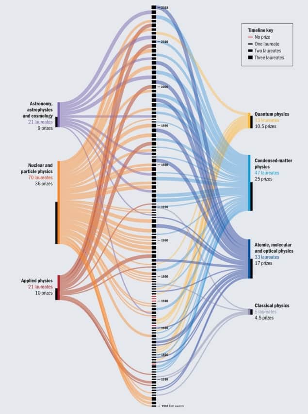
Basic science, of course, depends on photonics, whether it’s particle accelerators, telescopes or gravitational-wave detectors. Indeed, over half of all Nobel prizes in physics awarded in the last 25 years have been either related to discoveries in photonics or used photonics as a tool.
And don’t forget the whole world of quantum computing, communications and cryptography, which is either directly based on photonics or requires photonics to function. It’s an industry that’s really starting to take off. The London-based firm Orca, which won a business start-up award from the Institute of Physics in 2020, has just sold its first quantum computer to the UK Ministry of Defence.
Real-world benefits
Photonics is also helping the world reach net-zero thanks to highly efficient photovoltaic solar cells, while advanced LIDAR – combined with computer simulation – can boost the output of wind farms. Estimates by PLG suggest that photonics will increase the efficiency of new and existing wind turbines by 1.5–2%. With little additional cost, this will provide an additional 15 GW generating capacity globally by 2035 – saving more than £100bn (roughly equivalent to five Hinkley Point C nuclear-power stations).
Light is vital in medicine too. There’s laser corrective-eye surgery, while even high-street opticians these days use a vast array of photonics tools. During a recent eye test at my local branch of Specsavers, I got chatting to my optician, who didn’t seem to know much about the physics behind the Optical Coherence Tomography (OCT) system he was using, but was blown away by the images he could see. By imaging the back of the eye at different depths, opticians can use OCTs to safely spot a range of health and vision problems, often before they have become serious.
Optical fibre, optical amplifiers and atomic-clock traceable time stamps are all UK inventions. Secure quantum communications are being pioneered in the UK. In fact, I’d say Britain is uniquely positioned to be at the core of the next secure trusted telecoms revolution in 5G and 6G networks – and beyond. According to the PLG, by 2035 the UK will once again be a global provider of critical communications infrastructure.
All I can say is that if you didn’t know about photonics already, I hope you do now.
Condensed-matter physicists knew that CeRh2As2 was an unconventional superconductor, but they didn’t appreciate just how unconventional it was until an international team of researchers took a closer look at how it behaves in high magnetic fields. According to the latest findings from researchers at the Max Planck Institute for Chemical Physics of Solids (MPI CPfS) in Dresden, Germany and colleagues, CeRh2As2 is one of only a few materials to boast an odd-parity superconducting state – that is, one that is stable to magnetic fields applied in certain directions.
Superconductivity usually exists in two forms. The first is easily destroyed by the presence of a magnetic field and is said to have even parity – that is, the wavefunction of the superconducting state is symmetric with respect to an inversion point. The second is stable in magnetic fields applied in certain directions and has odd parity – that is, its wavefunction is asymmetric.
In materials with odd-parity superconductivity, the critical field at which superconductivity disappears should exhibit a characteristic angle dependence, explains study leader Elena Hassinger. Odd-parity superconductivity is, however, rare and only a few materials (including UPt3 and the ferromagnetic superconductors UCoGe, URhGe, UGe2 and UTe2) are known to have it – and none of them display the expected angle dependence.
Low- and high-field states
CeRh2As2 is a so-called heavy fermion compound that was recently found to exhibit two superconducting states: a low-field state and a higher-field one that appears when a magnetic field of 4 T is applied along a certain direction of the material’s crystal structure (the c-axis). In their work, Hassinger and colleagues showed that the angle dependence in CeRh2As2 is precisely that expected of the odd-parity state.
They obtained this result by measuring the material’s AC magnetic susceptibility, magnetic torque and specific heat as a function of temperature, applied magnetic field and different directions of the magnetic field with respect to the crystal axes. In these experiments, ultralow temperatures below 1 K and high magnetic fields of up to 36 T were required.
“We compared the resulting phase diagrams with a model by our international collaborators that contains both the even- as well as the odd-parity superconducting states,” Hassinger tells Physics World. “The model we used is simple yet powerful since it is based on the symmetry of the crystal and relies on a very limited number of parameters. It can reproduce our experimental results almost perfectly.
“Researchers have been looking for odd-parity superconductivity for a long time and CeRh2As2 allows us to investigate the properties of this type of superconductivity – namely the electron pairing mechanisms at play [that are] responsible for how superconductivity evolves,” she adds. “The material is also important for further understanding the interplay of superconductivity with the other ordered states that have been previously observed – for example, a quadrupole density-wave state and an antiferromagnetic state that appear at a similar temperature to the superconductivity.”
The light trap: The set-up comprises a partially transparent mirror, a thin, weak absorber, two converging lenses and a totally reflecting mirror. Due to precisely calculated interference effects, the incident light beam interferes with the beam reflected back between the mirrors, so that the reflected beam is ultimately completely extinguished. (Courtesy: TU Wien)
Physicists in Austria and Israel say they have developed an “anti-laser”, or “coherent perfect absorber”, that can enable any material to absorb all light from a wide range of angles. The device, based around a set of mirrors and lenses, traps incoming light inside a cavity and forces it to circulate so that it hits the absorbing medium repeatedly, until completely absorbed. This has the potential to improve various light harvesting, energy delivery, light control and imaging techniques.
The absorption of light is important in many natural processes, ranging from vision to photosynthesis, as well as in physics and engineering applications such as solar panels and photodetectors. Techniques to enhance light absorption in order to boost the efficiency and sensitivity of light-based technologies are highly sought after, but this can be challenging.
Stefan Rotter, a theoretical physicist at TU Wien, explains that it is easy to trap and absorb light with a bulky solid object, like a thick black woolly jumper, for instance. But most technical applications use thin layers of material. While these thin materials absorb some light, large parts of it pass through.
One reason that owls and other nocturnal animals have such good night vision is that they have a layer of reflective tissue, called the tapetum lucidum, behind their retina. Any light that passes through the thin retina without being absorbed gets bounced back and has a second chance to be captured. To improve such a system further you could add another reflective surface in front of the retina. Light would then bounce back and forth between the two mirrors, passing through the light absorbing surface multiple times. But it isn’t quite that simple.
For such a device to work, the front mirror cannot be perfectly reflective. It needs to be partially transparent so that light can enter the system in the first place. But then as the light bounces between the two mirrors some of it will be lost through the partially transparent mirror. When researchers tried to replicate such set-ups they found that they only work for specific patterns of light. While certain modes of light become trapped, repeatedly hitting the absorbing surface, other light, for instance entering the device at a different incidence angle or having a different wavelength, escapes.
Anti-laser: A perfect trap for light. (Courtesy: Hebrew University)
Now Rotter and his colleagues, also from The Hebrew University of Jerusalem, have demonstrated that a much more efficient light trap can be created if two lenses are placed in between the two mirrors.
The lenses are designed to guide the light so that it always hits the same spot on the mirrors. The interference effect that this creates prevents light from escaping through the partially transparent front mirror. Instead, it becomes trapped in the system.
“In practice, our design traps incoming light inside a cavity and forces it to circulate in a cavity, hitting the weakly absorbing sample again and again until it is perfectly absorbed, and all reflections are coherently destructively eliminated,” Rotter explains to Physics World. He describes the system as working like a laser in reverse. “Instead of having a laser gain medium convert electrical energy into coherent light radiation, our ‘time-reversed laser’ absorbs coherent light and converts it to thermal energy – and possibly in the near future to electrical energy.”
The front mirror in the researchers’ experimental set-up had a reflectance of 70%, while the back mirror had a near-perfect reflectance of 99.9%. For the light absorbing medium they used a thin piece of tinted glass with an absorption of around 15% – around 85% of light passes through it. They found that their device enabled the colour-glass to absorb over 94% of all light that entered the system.
The researchers also used a number of techniques to create rapidly changing, complex and random light fields. Even with these dynamic variations in the light source their coherent perfect absorber still enabled near-perfect absorption, they claim.
Rotter tells Physics World that their device has potential in a wide range of applications, particularly around optical energy harvesting and transmission. For instance, he says it might be possible to use it to charge the batteries of a drone from a large distance using a laser beam.
Composite layered 2D materials that are resistant to breaking and extremely stretchable. (Courtesy: Dong Li, Nanyang Technological University)
Natural layered materials such as bone and mother-of-pearl have many functions. Alongside helping organisms protect and defend themselves, some, such as the shells of marine animals, can also sequester carbon by combining proteins and inorganic composites. Researchers at Pennsylvania State University in the US have now engineered artificial versions of these composites inspired by the ring teeth of squid. The new structures are tough and extremely stretchy, and they might find use in applications such as robotics and flexible electronics as well as in carbon sequestration.
When carbon dioxide dissolves in the sea, it forms carbonate ions that can be taken up by microscopic creatures called coccoliths. These tiny animals build their shells, or exoskeletons, one layer at a time by converting carbonate to minerals like calcite or aragonite. Because biological organisms carry out this process of calcite transformation 1000 times faster than would be possible with purely chemical mechanisms (which normally take 10,000 years), study leader Melik Demirel explains that they could be used to sequester carbon from human-caused CO2 emissions.
Modifying repeating sequences
Artificial versions of these composite layered materials typically consist of atom-thick layers of a hard material like graphene or one of the MXenes (usually a transition metal carbide, nitride or carbonitride), separated by layers of a binding material. The strength of these composites stems from the properties of the interface layers and these can be modified by repeating sequences. In this way, a material can be made flexible and strong at the same time.
In their work, Demirel and colleagues studied the mechanical properties of atomically-thin inorganic layers interfaced with so-called tandem-repeat proteins by carefully controlling the latter’s molecular weight. The researchers explain that these proteins, which are known as squitex because they are inspired by the structure of squid teeth, adhere to the inorganic sheets via secondary beta- and alpha-helix structures. This mechanism is crucial as it gives the material a good degree of stretchiness and toughness.
The interface is important
The researchers found that the mechanical properties of their material cannot be explained by an existing model known as continuum theory. Their simulations, however, revealed that the interface is important: when the material contains a higher amount of the interface compound, it breaks in places when the material is under stress, but the material as whole does not break, explains Demirel. “While we expected it to become compliant, it is also super stretchy,” he says. “This finding opens up perspectives on failure mechanisms for composites that depend on interfacial rather than bulk properties.”
“Controlling interfacial strength ultimately engenders new design rules for nature-inspired composites,” he tells Physics World. “Although bare inorganic nanosheets are brittle, we designed flexible composites with proteins that are robust to flaws at critical structural length scales (of around 2 nm).”
With additional functionality such as electrical and thermal conductivity, the researchers say that their tough new materials could find applications in flexible circuit boards, wearable devices or other equipment that requires both strength and flexibility. The Penn State team, which reports its work in PNAS, is now working on scaling up the composites for potential applications in carbon sequestering. “We plan to aim for gigaton sequestration in the next 30 years,” Demirel reveals.
Researchers in France have created a new experiment that could improve our understanding of the dynamics of stellar and black hole accretion discs. Designed by Marlone Vernet and colleagues at the Sorbonne University of Paris, the experiment uses a combination of radial electric fields and vertical magnetic fields to contain a rotating disc of liquid metal. This allowed the team to observe how angular momentum is transferred within the disc – something that could provide insights into planet formation and the regions around black holes.
Accretion is the process by which a massive object such as a star or a black hole draws in gas and dust from its surroundings. The result is a circling accretion disk, with the gas and dust getting closer and closer to the massive object. In stellar systems, planets form within accretion discs and astronomers can study black holes by observing the radiation from their accretion discs.
For the dust and gas to move ever closer to the massive object, it must somehow lose angular momentum along the way. As a result, angular momentum must be transferred from inside an accretion disc to its outer edge. Exactly how this happens, however, remains a mystery. One possibility is that friction between the inner and outer parts of the part of the rotating disc transfers angular momentum outward – but the viscosity of discs seems far too low for this to occur.
Turbulent shear flows
A more plausible explanation is that the angular momentum transfer is enhanced by turbulent shear flows in the disc. But, despite decades of close examination with both telescope images and computer simulations, the mechanisms driving this turbulence are still unclear.
This has inspired astrophysicists to take to the lab and do experiments that are analogues of accretion discs. In a typical experiment a liquid is contained in the space between two independently rotating cylinders. Instead of gravity, the liquid is driven into motion through viscous friction with the two cylinders. By adjusting the rotation speeds of the cylinders, researchers can recreate the radial motions observed in real accretion disks – providing some insights into how angular momentum is transported outwards.
However, this setup is far from being an ideal analogue of astrophysical accretion discs. Not only is the liquid’s motion driven by a force unlike gravity, the fluid must also be vertically contained by upper and lower caps. Through viscous friction, these boundaries introduce secondary flows to the fluid, which do not have any counterpart in real accretion disc.
Limited secondary flows
In their study, Vernet’s team created a new experiment in which a liquid metal is driven into motion by a radial electric field. This field is generated by passing a current between an outer, ring-shaped electrode, and a central cylinder. Although the fluid is still vertically capped, the extent of the secondary flows is limited by a vertical magnetic field, which is created by coils placed above and below the disc.
In their experiment, the researchers were able to control both the liquid’s rotation speed, and its level of turbulence. By probing the liquid with sensors, they discovered that angular momentum was indeed driven outwards by turbulent flows inside the bulk of the disc. What is more, this occurred at very low values of molecular viscosity. This is very similar to observations of real accretion discs, where material loses its angular momentum and falls inwards – despite a clear lack of viscosity in the gas and dust.
Secondary flows are still present in the experiment, which means that the team was not able to fully simulate turbulent flows in accretion discs. With further improvements, however, the researchers hope that suspended liquid metal disks could soon enable astronomers to estimate the level of turbulence associated with the accretion disks they observe.
Cyber attacks on hospitals can have a devastating impact, especially for radiology and radiotherapy departments that are particularly reliant upon technology to function. A case in point is the nationwide cyber attack on Ireland’s public health services in May 2021, which interrupted scheduled radiotherapy treatments for some cancer patients for up to 12 days.
Following this incident, medical physicists at University Hospital Galway and the National University of Ireland Galway began to develop an in-house tool to help create revised radiotherapy treatment plans after interruptions occur. The tool – named EQD2VH – calculates treatment compensation plans and enables visual comparison of all plan options, as well as individual analysis of each structure in a patient’s plan. The researchers describe the new software tool in the Journal of Applied Clinical Medical Physics.
Radiotherapy is most commonly delivered over several weeks in a series of small radiation doses (conventionally 2 Gy) called fractions. Unplanned treatment gaps – whether due to cyber attacks, machinery breakdowns or patient illness – can cause significant setbacks. During such gaps, cancer cells rapidly repopulate in tumour tissue, resulting in a decrease in the radiobiological dose to the planning target volume (PTV).
Lead author: Katie O’Shea from NUI Galway. (Courtesy: Katie O’Shea)
To address this problem, EQD2VH uses dose–volume histogram (DVH) information extracted from original patient plans to perform treatment gap calculations. Lead author Katie O’Shea, of the National University of Ireland Galway, and colleagues explain that the software converts the physical dose in each dose bin (the range of dose between data points in a DVH) into the biologically effective dose (BED). This accounts for both repopulation effects in the PTV and the effects of sub-lethal damage to unrepaired normal tissue in organs-at-risk (OARs).
After modifying the BED conversion to account for dose variations in each structure, using a variable-dose method, the tool converts the BED for each structure into the equivalent dose in 2 Gy fractions (EQD2). This normalizes each treatment to conventional fractionation and makes it possible to sum plans with different fractionation schemes together. The resultant EQD2 -based DVH provides a 2D representation of the impact of treatment gap compensation strategies on both PTV and OAR dose distributions, as compared with the prescribed treatment plan.
To evaluate EQD2VH as a clinical decision-making tool, the researchers selected five high-priority patients with rapidly growing tumours whose treatment gaps should not surpass two days. This included four patients with head-and-neck cancers undergoing intensity-modulated radiotherapy and one lung cancer patient undergoing 3D conformal radiotherapy, who had treatment gaps of 12 or 13 days. These cases enabled the team to evaluate the use of EQD2VH for patients with both conventional (2 Gy) and non-conventional (2.2 Gy) fractionation and different treatment gap times (from nine to 46 days into their therapy).
The revised treatment plans for each patient were based on their original plans with either the dose-per-fraction or the number of fractions changed. O’Shea explains that each patient’s revised plan and schedule used a combination of twice-daily fractionation, weekend treatments and increased dose to the target volume to reduce the effects of cell repopulation.
The plans limited treatment to six fractions per week and precluded twice-daily fractionation on consecutive days. If the prescribed treatment could not be completed in the required time frame, the researchers investigated plans using hypofractionation (delivery of increased dose per fraction). They were able to visually and quantitatively compare various revised plans with the patient’s original plan to determine which would deliver the best dose to the PTV with the least dose to OARs.
The researchers note that the 2D representation of each individual structure in EQD2VH provides a more in-depth analysis than the Royal College of Radiologists (RCR)-recommended 1D point-dose calculation method that’s currently used to manage radiotherapy gaps. A 1D representation of dose distribution within a volume does not account for OARs typically having a non-uniform dose distribution and could overestimate OAR dose. In addition, the EQD2VH tool can create plans for any length of treatment gap, whereas the RCR guidelines are based on a standard gap of four to five days.
Additional benefits of the new tool include the ability to monitor each OAR in the patient’s plan to minimize further dose increases that could cause more acute toxicities. Users can also calculate the impact of different treatment gap durations on a patient’s treatment. This capability can help determine whether to transfer a patient to a different clinic if the gap at the scheduled clinic is too long or whether the patient can safely wait for treatment to resume.
EQD2VH can also account for changes in the overall treatment time and sublethal damage in normal tissue, which a commercial system may not be able to do. Most importantly, the tool does not need to be connected to hospital network to function – it can be used even if a hospital’s servers are still crippled by a cyber attack.
“We are still evaluating EQD2VH as a decision-making tool,” says principal investigator Margaret Moore from University Hospital Galway. “It is part of a current project reviewing patients receiving multiple re-treatments for palliative regimes where the dose-per-fraction is non-standard and where there may be a choice of fractionation schemes to consider. Converting treatment dose from a number of treatments with differing fractionations to EQD2 allows the radiobiological dose to target tissues and OARs to be accumulated for an overall dose overview, which can assist with the decision-making for the choice of further treatment.”
Across the globe, small and large firms alike are racing to develop and launch computing technologies based on quantum physics. While the basic principles have been in place for a few decades, researchers, industry and governments are all working towards building and scaling up practical quantum computers, with US tech firm Microsoft a key player.
Earlier this year, distinguished engineer and head of Microsoft’s Quantum team, Krysta Svore, delivered a keynote at The Economist magazine’s Commercializing Quantum event in London. She later caught up with Physics World to discuss the firm’s pathway towards a scalable quantum system – from topological qubits, to Microsoft’s Azure quantum cloud-computing platform and hybrid partnerships, to the quantum marketplace as a whole.
What is Microsoft doing in the quantum world right now?
One of the questions we’re considering is how to accelerate the journey to quantum advantage. What I mean by quantum advantage is, first of all, that we want to be able to solve problems that are meaningful and will help move our society forward. I have a daughter, and I want to change the future for her – I don’t want to leave her these Herculean challenges related to sustainability, climate change, energy and finding better ways to use the resources on our planet.
Quantum architecture Microsoft is developing quantum simulations and materials. (Courtesy: Microsoft Corp.)
With quantum computing, there’s hope that we can start to address some of these problems, but we’re not going to be able do it with a quantum computer as a standalone machine. To work out how to improve nitrogen fixation, or capture carbon dioxide and convert it to methanol, for example, you really need a hybrid solution, one that integrates quantum computing into a classical supercomputer. So that’s what we’re building at Microsoft with our cloud-computing Azure system. We’re aiming to produce a hybrid, heterogeneous, AI-powered, quantum-powered supercomputer that will bring forward solutions for these types of problems.
We’re also thinking about our software platform. We’ve been studying quantum algorithms for years, so we’ve taken what we’ve learned about how to optimize and compile them, and brought that knowledge to our platform. Right now, with Azure, you can try out small problems on a diverse set of real hardware that is supplied by our various partners. But you can also write applications, develop your code, decide how big a quantum computer you’ll need and work out how it will operate alongside a classical one. You can perform that integration and begin debugging the code now, because that code will remain valid as the machines scale up and become fully integrated with the cloud.
What’s your vision for how we get to a scale where we can do something meaningful with a quantum computer?
Microsoft has been thinking about scale from the beginning. We’ve studied quantum algorithms; we’ve studied the physics; we’ve worked on the whole system architecture from software to hardware. And what we’ve learned about scale is we need to be asking something different of our qubits and of our quantum machine.
Over decades of research, we’ve identified that a successful machine needs three key characteristics. First, it needs to be the right size. The qubit needs to be small enough that you can fit a million on a wafer, so that the machine is not going to end up being the size of a skyscraper. Next, it needs to be the right speed. The machine needs to be fast enough that when you run billions of operations, all of them can be complete in a matter of weeks, such that we don’t wait more than a month for the full end-to-end solution combining classical and quantum elements. Finally, we need a qubit that’s reliable enough as we scale up; one that won’t consume as many resources because we’re taking advantage of natural, intrinsic qubit properties to correct errors. That’s what will allow us to run billions of operations.
Key milestone Postdoctoral researcher Xiaojing Zhao works in Microsoft’s Quantum Materials Lab, where she and colleagues have recently observed a 30 μeV topological gap in indium arsenide-aluminium heterostructures. (Courtesy: Microsoft Corp.)
At Microsoft, we’ve identified and designed a qubit that we feel is just right on all those counts: the topological qubit. And within the last few months, we’ve shared some really exciting progress we’ve made towards creating this qubit. In essence, we’ve engineered devices that demonstrate this very elusive physics that’s been hypothesized about for a century, whereby so-called Majorana zero-modes emerge at the end of nanoscale wires. This is a signature of the type of physics we need to demonstrate a topological qubit, so it’s a very significant milestone both for science and for building the foundation we need to say, “Okay, we will reach a million qubits.”
Tell me more about this topological qubit. What’s it like when it comes to robustness? Does it need to be at cryogenic temperatures?
Yes, it operates at cryogenic temperatures, so in that respect it’s very much like some other qubits in the industry, such as superconducting qubits. It’s in a dilution refrigerator, and 100 mK is roughly the temperature range. In terms of robustness, this is something we’ll be working on for our next demonstration. What we’ve shown so far is the underlying fundamental physics and the properties of Majorana zero modes, but now we need to create a qubit out of that. By that I mean something you can perform operations with; something you can control and read out. Once we do that, then we’ll be able to measure it and say, “Okay, here’s its lifetime. Here’s how coherent it is.”
Cool idea Microsoft uses cryogenic devices such as dilution refrigerators to test its quantum technology at ultralow temperatures. (Courtesy: Microsoft Corp.)
But what’s wonderful about the topological qubit – and the reason we’re so invested in it – is that it has this natural error protection that we believe will help it scale. This property stems from the fact that the information the qubit encodes is, in a sense, split across four Majorana zero modes, one at each end of two nanowires. If nature tries to disturb just one of those Majorana zero modes, it won’t actually hurt the quantum state. In contrast, with a superconducting qubit, the quantum state is held at a single point, so if you get noise at that point, the state decoheres. Unlike that, we have a degree of error correction or fault tolerance that is built into our topological qubit.
At what point will you be able to run a problem on, say, Microsoft’s topological qubits and then repeat the experiment using a different type of qubit, and ensure we get the same output?
I love where you’re headed with this, and I’m happy to tell you that we can do that today. In fact, that’s part of the beauty of Azure Quantum – it offers people the chance to run the same code on multiple quantum computers, through the cloud service we have. You can write a single piece of code – maybe it’s a small instance of Azure’s algorithm, maybe it’s the quantum equivalent of “hello world” – and run it on hardware developed by companies such as Quantinuum and IonQ. Those are both ion trap platforms, but we’re also partnering with Quantum Circuits Inc. (QCI), which uses a superconducting qubit platform, and we have a silicon semiconductor-based superconducting qubit platform from Rigetti Computing and a neutral-atom quantum-processor platform from Pascal, both of which will be coming online soon.
So that’s five different quantum-hardware platforms available through Azure, and what’s really neat is the flexibility you have with the code. You can write your quantum algorithm in Q#, which is a high-level language for algorithm development. That would be my choice, but you can also come in with your own codes. For example, if you’ve previously run your problem on one of IBM’s devices and you have their Qiskit code already written, then you can simply execute that code too on our system. You can select any one of the five hardware platforms and it’ll compile the code for you to whichever “back end” you choose.
That means you can run the same application on all those back-end devices and see how it behaves. Because of course, these devices have different architectures, different connectivity and even different operation speeds and fidelities. Through Azure, you can learn all about those differences and similarities.
Are you planning to bring in additional hardware platforms?
Yes, we really believe in democratizing quantum computing by bringing the community in to grow the ecosystem. Much of our code and platform tools are open source, and as well as multiple hardware providers, we have a whole variety of simulators coming from our partners. These are programs that help you work out how your code will run on a given hardware platform, before you execute it. We also have what are called resource estimators, which you can use if you want to know how much an algorithm is going to cost you to run once the machines scale up, or how big a machine you’ll need.
A further exciting development is something we call Quantum Intermediate Representation (QIR), which allows you to take any high-level language (choose your favourite), map it to QIR and send it to any number of back-end providers. We see this as an important layer in the global software stack, as it’s something that facilitates an ease of translation or mapping onto different hardware.
Scalable qubits Microsoft is developing hardware, such as this semiconductor–superconductor heterostructure device, and software for its scalable quantum computer based on topological qubits. (Courtesy: Microsoft Corp.)
You can think of QIR as a universal mid-layer language that enables communication between high-level languages and machines. Many organizations have adopted it already. It’s been developed as part of an alliance through the Linux Foundation’s Joint Development Foundation. In fact, QCI, Quantinuum, Rigetti, Nvidia and Oak Ridge National Laboratory have all announced that they’re going to build their compilers through QIR.
And it’s all part of what’s called LLVM, which is a very popular classical compiler framework, so it allows you to leverage compilation and optimization tools from the classical computing industry. That really cuts the cost of writing translations. Otherwise, you would have to write new code for every language to every back end, which would be very expensive.
The quantum marketplace is at an interesting stage right now. It seems like every week, there are new quantum companies launching, but this massive boom phase is taking place before the technology has really established itself. Are you worried that there’s going to be a bust?
I believe that we need many, many minds at the table to advance this technology and to accelerate our progress. Traditionally, with this type of technology, advances would be measured in decades. Just think of the time it took to go from the invention of the transistor to having cell phones and iPhones. We don’t want that with quantum computing. We want to speed it up.
I believe that we need many, many minds at the table to advance this technology and to accelerate our progress
The good news is that we have huge advantages – we already have software and classical computers. Our predecessors didn’t have the ability to model what they were doing when they were moving from vacuum tubes to transistors to integrated circuits. They didn’t have classical computers to help them, whereas we have them at our fingertips. When I see the ecosystem grow – more companies, more start-ups, more university degree programmes – I view it as exactly what we need.
So instead of being focused on whether there will be a bust or a “quantum winter”, I focus on engaging those thought leaders, bringing those innovators to the table and democratizing quantum so we can get solutions out quickly. If we are showing progress, there will be no quantum winter, and I believe that we can make that progress across all areas, from devices and machines to software and apps.
Do you have a date in mind for “Q-day” – that is, the day the first practical computer comes online?
Quantum computers are already online. They’re in Azure and you can access them. But the rate at which we scale up and reach quantum advantage depends on everyone engaging and jumping in. At Microsoft, we’re running as fast as we can to scale up the machine and scale the platform, but we’re also dependent on people developing algorithms that require fewer qubits – perhaps by jumping in and using QIR to create a better compilation stack. Progress is about making a difference from both ends, improving the machine as well as bringing the cost of algorithms down. That’s what will change the timeline and hasten the day when we’ll see practical quantum advantage.