Elastomers that undergo large spectral shifts in colour when stretched very little have been developed by researchers in the US and South Korea. The material scientists say that these liquid crystalline elastomers with an unusually large Poisson’s ratio could have a variety of uses, from visual displays to smart windows.
Colour can be produced by the absorbance of light by dyes and pigments. Any wavelengths not absorbed reflect back and create the colour that we perceive. But colour can also be produced by nanoscale structures that scatter and reflect light. Indeed, such structural colours represent some of the brightest colours in the natural world.
There has been a lot of research interest in creating structural colours. As well as having the potential to be brighter, they offer other advantages over dyes and pigments. The nanostructures are more robust and longer lasting, and scientists claim they could be more environmentally friendly. They can also be engineered to scatter non-visible light, with reflection of infrared light having potential applications for passive cooling.
One challenge that material scientists have struggled with, however, is creating structural colouration that can change colour. One way to do this is to mechanically deform the material. The problem with this approach, says Shu Yang, an engineer and materials scientist at the University of Pennsylvania, is that you have to stretch it a lot. To shift from red to blue you would need to stretch the typical liquid crystal elastomers used by at least 40%, and in some cases by as much as 70%, she explains.
Now, Yang and her colleagues have managed to create an elastomer that can colour shift from near-infrared to ultraviolet wavelengths when stretched by less than 20%. They describe their work in Nature Materials.
Pressure-activated displays
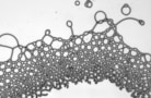
To create structural colour, the team used chiral nematic liquid crystalline elastomers. When these elastomers are produced, a chemical dopant encourages the molecules to form helixes. It is these helixes that create the structural colour, with the wavelengths reflected dependent upon their dimensions. If the material is stretched, the helixes compress and the material’s colour changes.
Yang tells Physics World that when one of her colleagues was playing around with the production of these liquid crystalline elastomers to improve the uniformity of the helixes and therefore the colour, they managed to produce a very soft material. It turned out that the elastomers the team created had an unusually large Poisson’s ratio. This means that when you stretch them in one direction, they compress much more than you would expect in the other plane. “That is why we are able to have a very large wavelength change at a small strain,” Yang says.
Next, the researchers used the elastomers to create pneumatically actuated displays. They 3D printed a plastic base containing circular cavities connected by air channels, and then sealed a layer of their new elastomer on the top, creating a series of colour “pixels”. Pumping air into the channels inflates the elastomer membranes, causing them to stretch and changing the colours that they reflect. The colours can be controlled by varying the pressure and the size of the cavities in the 3D-printed base.

The researchers demonstrated that an increase in pressure of just 9.6 kPa was enough to switch the wavelengths reflected by the pixels from near-infrared through red, green and blue to ultraviolet. They also showed that by using multiple air channels to activate groups of pixels, or individual pixels, they could create displays such as number countdowns.
Fast-switching structural colour could be used in low power video displays
As well as displays, the researchers suggest the material could be used for colour-changing soft robots and cryptic colouration, such as disruptive imaging and countershading. Yang says that because the material changes colour when subjected to a very small deformation, it could be used to create temperature, pressure or mechanical sensors.
Yang also suggests that the material may be suitable for building smart windows that reflect more infrared light as the ambient temperature rises. “That’s one of the interests, whether we can use the heat induced expansion of the air,” she tells Physics World.