Semiconductor metrology and standards will ensure the UK plays to its strengths

Smaller, faster, more efficient: the quest for relentless miniaturization has served the global semiconductor industry well – and, in fact, continues to do so, with the number of transistors on a microchip still doubling (per Moore’s Law) roughly every two years. Increasingly, however, applied scientists and engineers are redefining semiconductor progress along multiple axes of innovation.

The drivers? On the one hand, there is a convergence of new materials, advanced device concepts and heterogeneous integration (which combines different materials or technologies within one high-performance microelectronics package); on the other, the market-pull of disruptive technologies like AI and machine-learning, quantum computing and electrified transportation.

For the UK, “the opportunity is real and the direction is clear”, according to a new semiconductor metrology roadmap published by the National Physical Laboratory (NPL), the UK’s National Metrology Institute.

Following a three-year consultation exercise with around 500 semiconductor experts, the report – UK Priorities in Semiconductor Metrology and Standards to Drive Innovation and Growth – states that the UK must invest in foundational metrology and standardization capabilities to unlock commercial opportunities across the semiconductor supply chain.

“There’s been a gap in understanding – in policy circles and in industry – about the critical role that semiconductor metrology plays in defining what good looks like,” says Gareth Edwards, head of advanced manufacturing and materials strategy at NPL. “Publication of this roadmap is an attempt to reset the narrative by ensuring that metrology and standardization are treated as integral components of the UK’s semiconductor strategy, not as peripheral technical concerns.”

By shaping how emerging semiconductor technologies are measured, qualified and trusted, the roadmap argues the UK can help define the rules of future markets, support resilient supply chains and convert scientific excellence into sustained economic and strategic advantage.

“There’s a lot at stake here,” adds Edwards. “The countries that drive the conversation on standards development can ensure first-mover advantage for their domestic manufacturing base when it comes to roll-out and acceptance of new semiconductor materials, processes and products.”

Punching above its weight

While the NPL roadmap acknowledges that the UK is unlikely to become a leader in large-scale advanced silicon manufacturing alongside the likes of Taiwan, Korea and the US, the country has notable strengths that align well with the long-term trajectory of the global semiconductor industry.

NPL's Gareth Edwards

The UK’s academic and industrial R&D base, for example, consistently punches above its weight, underpinning world-class capabilities in compound semiconductors, materials science, photonics, power electronics, device modelling, semiconductor tooling and applied measurement science. Through organizations like NPL and BSI, the national standards body, the UK also has an unrivalled reputation for rigour and trust in metrology and standardization.

All of which matters even more given that next-generation semiconductor technologies are advancing much faster than the standards that govern how they are made, tested and integrated.

For context, mature silicon platforms are built upon decades of recognized best-practice and widely adopted specifications. Novel materials and device architectures, by contrast, often arrive without agreed performance metrics, standard test methods or even consistent terminology.

“This means that NPL, and other national metrology institutes like it, have significant work to do where new technologies have to compete or integrate with incumbent semiconductor products,” explains Sebastian Wood, principal scientist for semiconductor materials and devices in NPL’s electronic and magnetic materials group.

The NPL roadmap therefore lands at an apposite moment, setting out 12 metrology priorities to address the UK’s capability gaps in semiconductor technology and manufacturing (see “Made to measure: the path to next-generation semiconductors”, below).

Sebastian Wood

The roadmap’s call-to-action spans the full life-cycle of semiconductor innovation – from materials and structures, through process development and scale-up, to device and system performance – with the aim of exerting influence where global semiconductor markets are still evolving rather than competing where they are already mature.

“As a facilitator,” says Wood, “NPL’s role is to address these metrology priorities by mobilizing key stakeholders across the UK semiconductor ecosystem.”

Operationally, that means bringing together representatives from industry, academia and government to work on all aspects of semiconductor performance metrics, benchmarking and standards development; at the same time, reinforcing the UK’s voice in the European and international standards development organizations. “We want the UK to be a country that defines semiconductor standards, not one that must adapt to them,” he adds.

Joining the semiconductor dots

Encouragingly, the effort to translate the strategic vision for “UK Semiconductor” into economic upside is already under way. The official launch of the semiconductor metrology roadmap is a case in point, with a well-attended workshop at NPL’s Teddington campus in March yielding recommendations for delegates at all levels of the semiconductor supply chain.

The roadmap states that industry must engage earlier and more consistently in pre-competitive metrology and standards activity, recognizing it as an investment in market access and competitiveness. Academia, meanwhile, must align fundamental research more closely with the measurement and qualification needs that shape industrial adoption. Government, too, has a critical role to play by recognizing standards as strategic assets and through targeted funding for pre-competitive standards metrology and research.

“The metrology and standards roadmap offers a framework for a more joined-up innovation pipeline in semiconductor technology,” Wood concludes. “In this way, we will enable UK companies to not only translate their breakthroughs in basic science, but commercialize, scale and project them on global markets.”

Made to measure: the path to next-generation semiconductors

The NPL roadmap – UK Priorities in Semiconductor Metrology and Standards to Drive Innovation and Growth – sets out 12 priorities that must be addressed if the UK is to play a leadership role in the development of next-generation semiconductor technologies. The headline themes map versus the lifecycle of semiconductor innovation.

Materials and structures

  • Material property and measurement
  • Material quality and metrics
  • Defect metrology and classification
  • Metrology for complex 3D structures

Process development and scale-up

  • Defining manufacturing sustainability metrics
  • Process metrology and in-line inspection
  • Confidence in complex data flows and AI analysis
  • Heterogeneous integration standards

Devices and systems

  • Hardware security standards
  • Next-generation devices: performance testing
  • Package performance testing
  • Device reliability standards

Memory device breaks high-temperature performance record

Image showing the memristor chip against a background of a volcano spewing lava. There's a planetary rover in the foreground.

A memory device that can operate at temperatures over 700 °C could enable electronic systems to withstand harsh conditions with less need for cooling. The device, which is a memristor based on graphene, tungsten and a hafnium oxide ceramic, can store data for over 50 hours, has a working voltage of just 1.5 V, and is robust to more than 109 switching cycles. It also has a high switching speed of just tens of nanoseconds, according to its developers at the University of Southern California (USC), US.

“Our work provides one of the most critical electronic components – memory – for a wide range of applications, particularly in extreme environments,” says Joshua Yang, who directs USC’s Center On Neuromorphic Computing undeR ExTreme Environments (CONCRETE). “These include space exploration, deep-Earth drilling (for geothermal energy) and nuclear and fusion energy plants in which intense heat is generated.”

Heat-tolerant electronics could also dramatically reduce the need for energy-intensive cooling systems, cutting both power consumption and fan noise, Yang adds. “Our work also shows that these devices require significantly lower voltage and current to operate at elevated temperatures – meaning higher ambient temperature can actually improve energy efficiency of computing systems.”

A device to remember

Rather than being fixed, the resistance of a memristor (or memory-resistor to give it its full name) changes depending on the current or voltage previously applied to it. This means that specific resistances can be programmed into the devices and subsequently stored. Importantly, the “remembered” value of the resistive state persists even when the power is switched off, making it a non-volatile form of electronic memory.

Memristors are also capable of processing large amounts of data in parallel, making them faster and more energy-efficient than conventional memories for certain calculations such as matrix-vector multiplication. They are therefore useful for in-memory computer technologies, including those that are now routinely employed in artificial intelligence (AI) hardware.

An unexpected discovery

The memristor described in the new CONCRETE Center study consists of a hafnium oxide (HfO2) layer sandwiched between two electrodes: a tungsten one on top and a graphene one on the bottom. Tungsten has the highest melting point of any metallic element, and the study’s first author, Jian Zhao, notes that graphene (a sheet of carbon just one atom thick) can also withstand high temperatures without degrading. Nevertheless, Yang says they didn’t specifically set out to make a super-high temperature device.

“As often in science, this work originated from an unexpected discovery,” he explains. “We identified a material stack with significantly higher temperature tolerance while investigating something else completely – namely trying to build a different kind of device using graphene.”

Understanding why this stack could withstand such high temperatures and validating their hypotheses took considerable effort, Yang tells Physics World. The team used a combination of advanced electron microscopy, spectroscopy and first-principles calculations to work out the physical mechanisms behind the process, he adds.

The role of graphene

In conventional ceramic-based memristors, like those with a platinum bottom electrode, high temperatures cause the metal atoms from the top electrode to migrate through the ceramic layer until they reach the bottom electrode. When this happens, the two electrodes permanently connect and the devices short-circuit.

In the USC team’s memristor, though, this simply wasn’t happening. “Graphene puts an end to this process,” Yang explains. “Tungsten atoms still drift towards the graphene electrode as expected, but because of its surface chemistry and structure they cannot anchor onto it. These atoms therefore end up migrating away from the electrode, so avoiding short-circuiting and device failure.”

The researchers, who report their work in Science, say that one future research direction might be to search for materials that have a similar surface chemistry to graphene, but are easier to handle. Their next goal, which they acknowledge will be challenging, is to integrate their high-temperature memristors with logic devices (such as those based on SiC substrates) that can also withstand extreme temperatures.

To advance their memristor technology, Yang and his colleagues Glenn Ge, Miao Hu and Qiangfei Xia have founded a start-up company, Tetramem Inc., focused on developing memristor-based machine learning/AI accelerators. Though scaling up their devices will take time – the current examples were made by hand in the lab at the sub-microscale – Yang says that creating high-operating-temperature accelerators could enable intelligent computing in extreme environments, including space applications or datacentres.

How polarons travel through TiO₂

Complex oxide materials form a large family of compounds with highly tuneable electronic properties, making them important for electronics, magnetic devices, and energy technologies. In many of these materials, electrons interact strongly with lattice vibrations and form polarons, quasiparticles consisting of an electron plus the surrounding lattice distortion. Polarons play a key role in determining how materials conduct electricity, but they are difficult to study because theoretical modelling requires advanced methods to describe strong electron-lattice interactions characteristic of polarons, and experiments must be performed on ultraclean samples to reveal intrinsic behaviour.

In this work, the researchers combine experimental and theoretical approaches to study polarons in TiO₂, a material that is ideal for this purpose because it has a simple crystal structure, well‑known phonon modes, well‑characterised defects, and strong, reproducible electron-phonon coupling. They use a state of the art simulation method called first‑principles electron‑phonon diagrammatic Monte Carlo (FEP‑DMC), which accurately predicts polaron formation and transport. The calculations predict a room temperature mobility of around 45 cm² V⁻¹ s⁻¹ and a characteristic temperature scaling of μ ∝ T⁻¹·⁹, while also revealing microscopic details of polaron structure, phonon cloud distribution, and lattice distortion that experiments alone cannot access.

Lead researchers Marco Bernardi (left) from California Institute of Technology and Bharat Jalan (right) from University of Minnesota

The team then grew ultrahigh‑quality TiO₂ thin films with controlled oxygen vacancies using hybrid molecular beam epitaxy, achieving record high electron mobility in excellent agreement with the theoretical predictions. Microscopy and spectroscopy measurements show that oxygen vacancies act as intrinsic n‑type dopants and strongly influence low‑temperature transport, including in‑plane resistance anisotropy and signatures of the Kondo effect.

Together, these results provide the most detailed picture to date of how large polarons move in TiO₂ and demonstrate that the theoretical method is a reliable predictive tool for polaronic materials. This unified framework will help guide the design and engineering of improved electronic and energy materials in the future.

Do you want to learn more about this topic?

Review Phonons and thermal transport in graphene and graphene-based materials by Denis L Nika and Alexander A Balandin (2017)

When Fermi arcs flip, the current flips

Weyl semimetals are quantum materials in which electrons behave as if they are massless, moving with a linear energy-momentum relationship similar to photons. These materials also host Weyl fermions with a built‑in chirality, meaning their spin and momentum are locked in either a left‑ or right‑handed configuration.

A distinctive feature of Weyl semimetals is the presence of Fermi arcs which are surface electronic states that connect projections of bulk Weyl nodes. Because these arcs inherit the chirality of the underlying Weyl fermions, their motion is directionally biased and highly sensitive to the surface environment. This makes them promising for surface‑state engineering in topological devices.

The researchers show that the surface of the Weyl semimetal Co₃Sn₂S₂ can generate a strong, tunable second‑order nonreciprocal electrical response, which depends sensitively on the surface termination and can be further controlled by adjusting the surface potential. Crucially, when the Fermi arcs undergo a Fermi arc Lifshitz transition, a change in how the arcs connect across the surface Brillouin zone, the nonlinear current reverses sign. This sign flip arises from the chiral nature of electron velocities on the arcs.

The work demonstrates that measuring nonreciprocal transport provides a direct and experimentally accessible fingerprint of Fermi arc topology, offering a practical route to track and control surface states in Weyl semimetals without relying on complex surface‑sensitive probes.

Read the full article

Nonlinear transport fingerprints of tunable Fermi-arc connectivity in magnetic Weyl semimetal Co3Sn2S2

K X Jia et al 2026 Rep. Prog. Phys. 89 020503

Do you want to learn more about this topic?

Recent progress on correlated electron systems with strong spin–orbit coupling by Robert Schaffer, Eric Kin-Ho Lee, Bohm-Jung Yang and Yong Baek Kim (2016)

Decoupling electrical and thermal mechanisms could optimize brain tumour therapy

Effects of decoupled electrical and thermal fields on cell morphology and viability

A non-invasive cancer therapy known as tumour treating fields (TTFields) uses low-intensity alternating electric fields to inhibit cancer cell division and cause cell death. A new study providing fresh insights into how the applied electric fields kill cancer cells could help optimize future treatment of the brain cancer glioblastoma (GBM).

Most patients with GBM will have surgery to remove as much of their tumour as possible, before undergoing radiotherapy and chemotherapy. For newly diagnosed or recurrent GBM, tumour growth or spread can sometimes be slowed by adding in TTFields treatment. TTFields directs low-intensity (1–3 V/cm) alternating electric fields through the scalp to the tumour via insulated ceramic transducer arrays. The 200–300 kHz frequencies precisely target the rapidly dividing GBM cells, creating biophysical forces that disrupt cell division.

Simultaneously, the interaction of the electric fields with local conductive biological tissue heats those areas to between 38 and 39.5°C. While careful thermal management is required to prevent this “intrinsic mild hyperthermia (iMH)” side effect from injuring the scalp, studies in pancreatic cancer models have shown that deliberate application of additional hyperthermia in combination with TTFields can enhance cytotoxicity and inhibit cell migration. In this latest study, a team of researchers, led by Aili Zhang from Shanghai Jiaotong University in China, investigated whether the intrinsic heating during TTFields treatments for GBM could be optimized to produce similar advantageous effects.

“Our initial interest was to understand the biological effect of the electric field itself to find out why TTFields therapy works for some people but not for others,” explains Zhang. “As we looked more closely, we found that applying the field inevitably generates heat, which makes it difficult to distinguish the pure electrical effect from the accompanying thermal effect.”

That problem led the team to focus on electrothermal decoupling, in other words, separating the electrical and thermal components: an important step for clarifying the exact mechanism by which the GBM cancer cells are killed and for developing possible treatment optimization protocols.

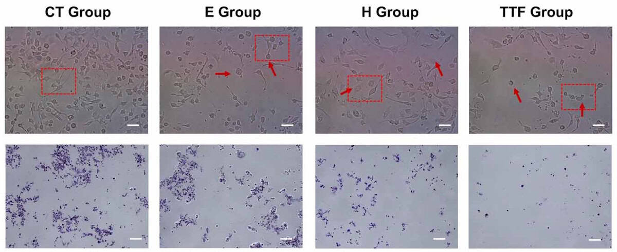
As detailed in Physics in Medicine & Biology, Zhang and colleagues used numerical simulations to help them create an in vitro experimental platform capable of decoupling TTFields’ electrical and thermal components. The 230 kHz, 2 V/cm electric fields were applied via custom-designed, conductive, 2 mm-wide titanium electrodes created to safely enable precise delivery to in vitro wells containing murine GBM cells.

The team used numerical modelling to estimate temperature, and to optimize the electrode geometry and spacing such that a stable and sufficiently uniform electric field could be generated in the central monitoring area where the cells were being analysed.

“Just as importantly, the modelling told us how much intrinsic heating would be generated during TTFields exposure and how to compensate for it. Based on those results, we could set the incubator conditions to create a pure electric condition, a pure thermal condition and the combined TTFields condition,” explains Zhang.

Their results revealed that while the electric field component of TTFields was more closely associated with suppressing the proliferation and migration of cells, the decrease in both cell viability – thanks to elevated levels of calcium ions which help mediate cell death – and metabolic activity was primarily due to the thermal iMH.

“We became genuinely excited when the decoupled experiments started to show that the electric and thermal components were not simply producing the same biological effect at different intensities, but were contributing in clearly different ways,” Zhang tells Physics World.

“That was a significant moment because it suggested that the heat generated during TTFields should not be viewed only as an unwanted by-product, but as a potentially meaningful therapeutic component,” she continues, explaining that, importantly, “the combined TTFields condition performed better than would be expected from a simple additive effect”. This electrothermal synergy, the researchers believe, comes from the thermal component sensitizing the cells by increasing membrane vulnerability and disturbing calcium homeostasis, thereby allowing the electric field to more effectively drive cell death.

Next, Zhang plans to confirm the synergistic effect at the molecular level and “systematically examine how the electrothermal interaction changes across different TTFields frequencies, field strengths and thermal conditions for different GBM human cell lines”. The ultimate aim is to find the “optimized treatment protocol” for glioblastoma. Understanding such heating effects could also help optimize other medical treatments such as cardiac ablation, she adds.

Proton therapy could improve treatment options for dangerous heart rhythm disorder

A first-in-human study from researchers at the Mayo Clinic has shown how proton therapy could provide a new treatment option for patients with hard-to-treat ventricular tachycardia (VT), a life-threatening heart rhythm disorder. In the small group of patients examined in this early feasibility study, the treatment led to a 79% reduction in VT episodes.

VT is a type of abnormal heartbeat in which faulty electrical signals in the ventricles cause the heart to beat too quickly, meaning that it can’t pump enough blood around the body. Treatments include antiarrhythmic drugs or the use of catheter ablation to destroy the areas of myocardium (cardiac muscle) responsible for the abnormal signals. Sufferers can also be fitted with an implantable cardioverter-defibrillator (ICD) that automatically delivers a shock to reset the heart’s rhythm during a VT attack.

Some patients, however, don’t respond to conventional therapies, including antiarrhythmic medications and catheter ablations, and ICD shocks can significantly impact quality-of-life. For these cases, cardiac radioablation – which uses external-beam radiotherapy to target the problematic myocardium – is under investigation as an alternative, catheter-free treatment for VT.

Previous clinical studies of cardiac radioablation have employed photon-based irradiation, which can expose surrounding cardiac tissue to low-to-moderate radiation doses. Beams of protons, on the other hand, deposit almost all dose at a defined depth (the Bragg peak) and could enable more precise targeting with reduced irradiation of nearby healthy tissue.

“The main motivation for investigating cardiac radioablation is to improve upon the limitations and suboptimal outcomes of catheter ablation of VT in some patients,” explains lead investigator Konstantinos Siontis. “The motivation specific to protons is the potential dosimetric advantage, allowing more precise myocardial targeting while minimizing radiation to surrounding cardiac and extracardiac structures compared with photons.”

In this new study, reported in Heart Rhythm, Siontis and colleagues used proton-based cardiac radioablation to treat seven patients with advanced cardiomyopathy (disease of the heart muscle) and recurrent VT despite drug treatment and previous catheter ablations.

First-in-human investigation

To define the target myocardium for radioablation, the team integrated data from multiple imaging modalities (primarily MRI, plus CT) with information from electrocardiogram (ECG) and electrophysiology mapping originating from the patient’s prior invasive ablation procedures. The CT images were then used to contour the target and organs-at-risk (OARs) and for treatment planning.

The researchers designed treatment plans to deliver a single 30 Gy fraction of expiration-gated intensity-modulated proton therapy to the cardiac internal target volume (ITV, the target myocardium expanded to include cardiac motion) while sparing surrounding OARs. They point out that, due to safety uncertainties in thisfirst-in-human study, they took a generally conservative approach to target definition. In all patients, at least 90% of the ITV received 100% of the prescription dose, while a median of 96.2% of the ITV received at least 95%. Importantly, only 4.3% of non-target myocardium received a dose of 20 Gy or above.

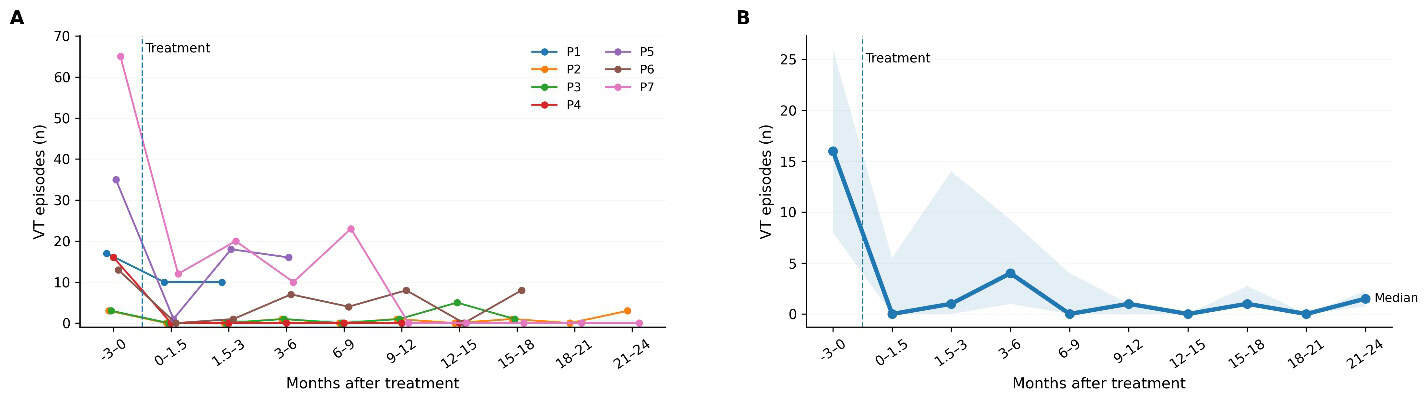
VT episodes before and after treatment

After treatment, the investigators performed follow-up evaluations for up to two years (median 514 days). Most patients experienced recurrent VT during this time, although less frequently than before the radioablation. Across all patients, the rate of VT events declined from 7.24 per patient-month in the three months before treatment to 1.52 per patient-month afterwards – corresponding to a 79% reduction in VT event rate. None of the group experienced serious treatment-related side effects and key heart function measures remained largely stable.

All patients in this study had advanced structural heart disease with severely reduced ventricular function and recurrent VT, putting them at high risk of both arrhythmic and heart failure-related mortality. In line with this profile, two patients required heart transplantation (at 66 and 514 days after treatment) and three died (at 155, 502 and 529 days), due to progressive heart failure.

“This early feasibility study demonstrates that proton cardiac radioablation for refractory VT can be safely planned and delivered with encouraging reductions in arrhythmic burden and no clear treatment-related toxicity,” the researchers conclude. “These findings support the feasibility of proton-based cardiac radioablation and justify further investigation,” they write.

Siontis notes that alongside the emergence of cardiac radioablation techniques, catheter ablation tools are also constantly improving. “Radioablation is unlikely to replace catheter ablation broadly, but it could become an important complementary or salvage option for patients with refractory VT who are poor candidates for invasive procedures,” he tells Physics World.

The team is now planning a larger prospective trial to better define the safety, efficacy and optimal targeting. “We are also investigating improved radiation delivery techniques, such as optimizing treatment planning around cardiac motion,” says Siontis. “In parallel, we continue to investigate photon radioablation in a pivotal randomized trial (RADIATE-VT), while we also offer proton therapy as a compassionate use option for patients in need in our clinical practice.”

The strange metaphor of Euglena’s tail

Quantum mechanics is so full of strange phenomena that it’s not surprising that physicists have had to dream up some vivid metaphors to explain them. Who can’t help but think of cats in boxes when contemplating superposition or balls of jumbled yarn when musing over entanglement? Like all metaphors, these use familiar experiences to help understand the unfamiliar.

Metaphors come in many different types. “Love is a rose”, for instance, is a “filtrative” metaphor, in which a secondary subject (a rose) guides us how to perceive another, primary subject (love) by drawing our attention to key features.

In a “creative” metaphor, however, the secondary subject eventually becomes the technically correct term for the primary subject. This has happened over and over again in quantum mechanics: entanglement, superposition and spin are all examples.

A third kind is a “perceptual” metaphor, which seeks to recast our overall view of something. A good example is physician Lewis Thomas’s remark that the Earth is “most like a single cell.”

But one extraordinary metaphor proposed 10 years ago by Christopher Fuchs, a physicist at the University of Massachusetts Boston, involves a type of algae known as Euglena. Fuchs decided to invoke this single-celled, biological organism to help understand not just one quantum-mechanical phenomenon but possibly the deepest mystery of all: the relationship between quantum formalism and the world around us.

Subjective matters

Ever since Werner Heisenberg and others developed quantum mechanics more than a century ago, physicists have been debating what it means and what it says about the world. Over the years, there have been many different points of view, or “interpretations”, of quantum mechanics, but they all fall into two main camps.

One set claims that the formalism of quantum mechanics quantifies some actual, objective structure that existed even before humans and is independent of what we do. Another set of interpretations treats the formalism like a tool that lets humans make predictions about the world. In philosophical terms, the former interpretations are “ontological” and the latter “epistemological”.

Fuchs and a loose conglomerate of physicists and philosophers, however, have been advocating an entirely different approach, known as QBism. It says that any measurement we make – whether determining the spin of an electron or stamping our feet on the ground – is a new creation; it’s an experience that never existed in the world before. Quantum states aren’t therefore real states of affairs in nature but subjective probabilities we assign to our interactions with the world.

Subjective probabilities aren’t as strange as they sound, simply describing a user’s degree of belief about an individual event. Objective interpretations, in contrast, see probability distributions as physical. QBism’s conclusion that many pieces of the formalism are subjective simultaneously distances our subjective control over nature. For a one-horse race, I can predict the winner with certainty, but nevertheless, the race can still get washed out by rain. Even if I make a prediction with certainty about an event, nature can throw us a curveball and do otherwise.

For Fuchs and his supporters, quantum theory is therefore an appendix to Bayesian probability theory. Originally developed by the British philosopher and statistician Thomas Bayes in the 18th century, it evaluates a user’s judgment about how likely an outcome is (such as whether a horse will win a race) rather than being about pre-existing states of affairs (such as passively recording the speed of particles in a gas).

Fuchs calls his interpretation of quantum mechanics QBism as it derives from the term “Quantum Bayesianism”. Quantum mechanics, according to Fuchs, is a “user’s manual” that “anyone can pick up”, devised by experienced players to guide individual experimentalists to make wise bets on measurement outcomes.

Subjective interpretations of quantum mechanics treat the formalism as something for individuals to use and apply for all kinds of physical phenomena

The key point is that while quantum state assignments are subjective, the rules underlying them aren’t. They have been analysed, evaluated and corrected over time by communities of physicists. Subjective interpretations of quantum mechanics treat the formalism as something for individuals to use and apply for all kinds of physical phenomena.

Enter Euglena

If you’re struggling to get your head around all of this, that’s where Euglena comes in. It’s a single-celled freshwater algae, roughly 50 microns long, that has a long whip or “flagellum” that can sense nutrients and propel the organism towards the food. The tail, which is the product of many years of evolution, helps only the organism to which it is attached. However, by studying it, we can learn not just about an individual Euglena but also the wider environment in which it moves.

The metaphor of Euglena’s tail therefore does two things. First, it expresses the idea that quantum formalism is a manual – a means to get around in the world. Second, it says something about how we interact with the world.

Each organism uses its inherited tail, constantly tested and improved by a community of others, to “guess” how to get around in its environment. But each time the organism does, it encounters something in the environment it never did before.

Euglena’s tail can, in other words, help us to explain why quantum mechanics can be both a single-user theory and the product of extensive study. “By dissecting it,” Fuchs wrote in a 2016 arxiv preprint (1601.04360), “you can learn something about the world that all of us are immersed in.”

Like all metaphors, however, Euglena has its shortcomings.

Imagine standing above the Euglena and observing it through a microscope. It would be perfectly reasonable to say that “there is” an environment that the organism senses “thanks to” the whip. We might also conclude that what a Euglena encounters is objective, independent of its presence, and could be predicted by the organism, provided it had enough data and processing ability.

But all this assumes we are looking down from above to adopt a point of view completely detached from Euglena and its environment; we, as researchers, are outsiders. The Euglena organism itself is different. It has no such outside standpoint and each move is creative, encountering a fresh environment.

Physicists have no external standpoint from which to look down on the world

Now here’s the key point of the metaphor. Quantum physicists, too, cannot become “outsiders”. They have no external standpoint from which to look down on the world. They have the quantum formalism, but it’s a guide to what we find in our fresh encounters with the world.

The critical point

Fuchs’s Euglena metaphor has a much broader scope than the other scientific metaphors mentioned above. It is not so much about comparing a piece of the organism to quantum mechanics, but a way of comparing an organism’s adaptation to its world to the experimentalist’s user-manual; in turn, it becomes a story about what the world is.

The Euglena’s tiny whip is a way to grapple with the ontological lesson of quantum mechanics. You might, in fact, call it an “ontologizing” metaphor.

Robert P Crease  (click link below for full bio) is a professor in the Department of Philosophy, Stony Brook University, US, and Gino Elia is a philosopher of physics who is spending 2026–27 at the Ludwig Maximilian University of Munich, Germany, e-mail gino.elia@stonybrook.edu

Quiz of the week: how far can new tiny knotted fibre leap into the air?

Fancy some more? Check out our puzzles page.

Tiny knotted fibre leaps into the air like a springtail bug

Researchers at the University of Pennsylvania and the University of California, Los Angeles, have created a tiny, soft knot-like fibre that can jump metres into the air.

The fibre is less than a millimetre thick, and a few millimetres long and contains a Kevlar core surrounded by a shell of liquid crystal elastomer (LCE).

The Kevlar provides strength and stiffness while the LCE adds some flexibility and responsiveness.

“People think of a knotted fibre as something passive,” says Shu Yang from the University of Pennsylvania. “But if you design the elasticity and materials carefully, the knot itself becomes an active system.”

When the fibre is knotted it behaves like a spring held in place by a latch, which can be undone via changing the temperature.

When the temperature is increased to 60–90 °C, the LCE shell contracts and untwists, which loosens the knot just enough to trigger an abrupt untying.

All that stored elastic energy then converts into kinetic energy, propelling the fibre almost 2 m into the air – a feat comparable to the jumping capabilities of a springtail bug (for a video see here).

Changing the knot’s topology and the materials used allows the researchers to tune how the fibre moves after take-off. For example, a simple overhand knot results in a flipping motion while a figure-eight knot leads to the fibre spinning.

Inspired by the flight of Maple seeds, the team attached a thin, leaf-like appendage to the fibres, finding that where the wing is positioned on the knot resulted in the fibre landing far away or curving backwards towards its starting position.

Given the fibres can be activated with temperature, the researchers think the robot could find applications in agriculture and reforestation.

“We often start by exploring interesting phenomena,” adds Yang. “Then we ask how far we can push them and whether they can solve real problems.”

Caffeine kick: can you solve our crossword on coffee physics?

See how much you know about the subject by trying our interactive crossword. Most of the clues are based on the article, but there are a few additional brain teasers thrown in. If you’re feeling stuck, check out the “assist” menu for help.

Copyright © 2026 by IOP Publishing Ltd and individual contributors