Black holes are nature’s fastest data-scramblers, and new research suggests that secrets thrown into them may be more secure than previously thought. In a paper published in Physical Review Letters, researchers at Los Alamos National Laboratory (LANL) in the US show that once a message has been scrambled by a black hole or another system with similar properties, not even a quantum computer can put it back together.
Scramblers are quantum systems that take local information and spread it across the entire system, generating quantum entanglement between distant regions. They crop up in various contexts in physics. While black holes are perhaps the most famous example, scramblers also exist in simple systems such as spin chains – 1D arrangements of quantum particles with coupling between nearest neighbours – and in “strange” metals, in which resistivity depends atypically on temperature.
Although the scrambling process is deterministic – a fixed input yields a fixed output – scrambling systems can give rise to tremendously complex behaviour, distributing information in seemingly random fashion. This emergence of apparent randomness is known as quantum chaos, in analogy with classical chaos theory, where similarly simple systems produce equally intricate dynamics.
A shred of hope for message recovery
Physicists working at the intersection of quantum mechanics and gravity are interested in scramblers in part thanks to the so-called black hole information paradox. The paradox revolves around the ultimate fate of information that falls past the event horizon and into a black hole: after a message is scrambled across the surface of a black hole, is its information trapped in the black hole forever, or does it somehow manage to escape? One school of thought holds that information does escape from black holes in the form of photons emitted via a process known as Hawking radiation. This theory received some corroboration in 2019, but the jury is still out.
Studying scramblers Lead author Zoe Holmes is a postdoctoral scholar at Los Alamos National Laboratory. (Courtesy: Zoe Holmes)
In 2007, while investigating this paradox, physicists Patrick Hayden and John Preskill came up with a thought experiment. Assuming that black holes do encode information in Hawking radiation, they showed that when a message is sent into a black hole, its pieces can be rapidly recovered by capturing a few of the emitted photons – a process akin to recovering the slices of a shredded document from the heat given off by the shredder. However, while the black hole’s scrambling behaviour makes such a recovery possible, the Hawking radiation alone doesn’t tell you how to unscramble a scrambled message. Other approaches are needed to, in effect, reassemble the shredded document from its paper strips.
Scramblers beset by barren plateaus
Enter machine learning algorithms. These powerful pattern-identifying tools “learn” how to best approximate a physical system by comparing outputs of the real system to their own outputs (given the same inputs for both), tweaking their internal model, and then rinsing and repeating until reality and approximation align. The central quantity in this learning process is a mathematical quantity known as the cost function, which captures the degree of deviation between the model and the real system.
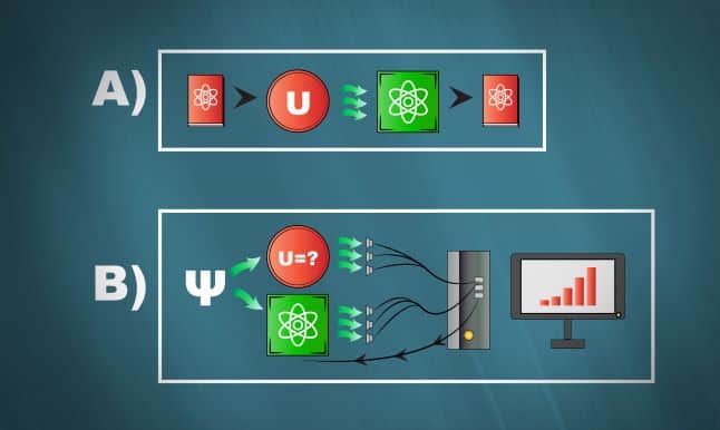
Scrambler schematica A scrambler, represented by unitary U, disperses input information. b A proposed protocol for learning how to unscramble a scrambled message using a quantum computer. The researchers found that this protocol suffers from the problem of barren plateaus. (Courtesy: Los Alamos National Laboratory)
In classical machine-learning methods, the cost function is like a mountain range, replete with peaks and troughs that represent its higher and lower values. Minimizing the cost function – and learning a model for the system – is like finding a descending path and following it down to base camp. When the model is a quantum system modelled on a quantum computer, however, the cost function landscape isn’t always so rich. In fact, the LANL researchers showed that when the algorithm is asked to model a scrambler, it suffers from the problem of “barren plateaus”. “The cost function is essentially flat everywhere, with a needle-sized hole that is the base,” says Zoe Holmes, a postdoctoral scholar at LANL and lead author on the paper.
This absence of features in the cost function renders quantum machine learning ineffective, because finding the “hole” from a random starting point within the landscape is almost impossible without a downward path to follow. “If you’re learning using a cost function evaluated on a quantum computer, no matter how many training pairs you have, you won’t be able to learn the scrambler,” Holmes says, “at least without prior knowledge”. This flaw rules out the possibility of reconstructing a message, which would entail inverting the scrambling process.
A hard lesson to learn
The LANL researchers conclude that even if the pieces of a scrambled message are known, putting them back together poses a problem that quantum computers cannot help us solve. “You could perhaps (ambitiously!) try to use the fundamental physics of the black hole to put a message together,” says Holmes, cautioning that no such method is currently known, “but any learning method looks pretty doomed”. Nature, it seems, is a pretty good confidant.
Water molecules on cold surfaces require some additional heat before they can form ice, an international research team has discovered. Their novel experiment found that water molecules on a cold graphene surface initially repel each other, until additional energy allows them to reorient themselves and form electrostatic bonds. The findings fill an important gap in our knowledge of ice formation – and could lead to new ways of controlling the freezing process.
When liquid water encounters a cold surface, ice can quickly form through the process of nucleation whereby individual water molecules coalesce bond with each other to form ever larger solid crystals. While nucleation has been widely studied on the macroscopic scale, it is difficult to study on the molecular scale because it occurs on a timescale of tens of picoseconds, which is too fast for conventional instruments.
Now researchers led by Anton Tamtögl at the University of Cambridge (now at the Graz University of Technology) and Marco Sacchi at the University of Surrey have observed nucleation on the molecular scale using a technique called helium-3 spin echo. First developed at Cambridge, the technique involves scattering a beam of spin-polarized helium atoms from molecules on a surface. The atoms arrive at the surface in wave packets that are separated by regular time intervals on the picosecond scale. The motions of molecules on the surface causes differences in the phases of successively scattered wave packets, which is detected using a spin-echo technique.
Dipolar repulsion
The experiments revealed that water molecules initially attach to a cold graphene surface with the same orientation: the two hydrogen atoms are close to the surface while the oxygen atom is elevated above the surface. Water molecules are electric dipoles (the oxygen end is negatively charged, and the hydrogen end positively charged) so there is a dipolar electrostatic repulsion between these similarly oriented molecules and this suppresses nucleation. The team found that this barrier can only be overcome by heating the molecules to change their orientations so that their oppositely charged poles can attract each other, initiating nucleation.
To understand their observations, Tamtögl and colleagues did computer simulations of the interactions between adsorbing water molecules at varying energies. As they hoped, altering the amount of applied heat switched nucleation on and off – agreeing with experimental observations.
The team’s results could lead to new techniques for controlling ice formation on wind turbines, aircraft and telecommunications equipment. They could also provide important insights into ice formation and melting in glaciers and ice sheets – allowing researchers to better quantify the effects of climate change on the cryosphere.
We’re a quantum computing software and algorithm company, and we’re just over six and a half years old, so we’re in early adolescence. We’re trying get the most out of quantum computers both now and in the future, and in that respect, there are two sides to the coin. On one side, we work with the hardware companies to make sure that whatever hardware they’ve got is put to best use. There’s a long history of this in classical computing, where for 70 years we’ve had great algorithms and great software making hardware even better. And then on the other side of the coin, we work with users – people who have problems that might be solved by quantum computing. That side is obviously in its infancy, but what we do in these early days is to make sure that whatever is available can be useful.
You’ve developed software for applications in quantum chemistry and you’re working with PhD students in pharmaceuticals. Can you tell us more about that?
The point that’s probably worth making first is that there’s an informed consensus (and it has been an informed consensus for some time) that one of the great applications for quantum computers lies in materials discovery. At the most profound level, discovering new materials is a quantum mechanical simulation because it’s ultimately about understanding the stability of different molecular systems.
At Cambridge Quantum, we decided that this was extremely important a while back, when we decided to look at some of the biggest problems the world might face. One example of such a problem might be drug discovery in fields such as Alzheimer’s research, where there are few treatments available. Another might be carbon sequestration, where a material that could lock away carbon safely would be hugely beneficial. Other examples might include extending battery life, developing better surfactants for hydrocarbon extraction, or making refrigerants that don’t impact on the ozone layer.
We looked at a handful of these big problems, and we decided to partner with clients who knew more than anybody else about these areas. We’ve now got an enterprise-level software platform for that partnership, and it is beginning to do things that people have been dreaming about doing with quantum computers for a long time. It’s really exciting.
There is still a lot of academic work to be done, so we are working with (for example) the pharmaceutical firm GlaxoSmithKline in sponsoring PhD studentships. But the spectrum of what we do includes real applications, too. In 2020 we announced that we would be working with the oil company Total on a carbon sequestration solution based on metal-organic frameworks.
You’ve got an agreement with Honeywell for access to its quantum computer. Do your customers use other quantum computers as well?
Quantum computers are still somewhat restricted in their availability and, frankly, in their performance. But this will change quickly. Already, over the course of the last year, the changes are incomparable. Large corporations now have the resources and relationships to access machines directly, and those machines are available from IBM, from Honeywell, and from other companies as well. It’s also now possible to subscribe to these machines, because some of the big cloud providers (Amazon Web Services and Azure are two examples) have taken initial steps towards offering what we might describe as quantum processing units alongside regular high-performance computing. Those early access agreements are now available for subscription, sometimes on a daily or even an hourly basis. And then beneath all of that, there is a clutch of start-ups like IQM in Finland, Alpine Quantum Technologies in Austria and Oxford Quantum Computing in the UK that are all on a very steep trajectory. Their processors will be available in a variety of ways.
All of this means that a large corporate entity has a variety of ways of accessing quantum processors, and what we do is to pull all of that together. We have two distinguishing features. We have a software development platform called Ticket that is platform-agnostic, meaning that people can reserve the right to use any machine. We also have access to the Honeywell machine, and we’re a client of the IBM quantum computers (of which there are rather more at the moment than there are of the Honeywell machines). So we have access to at least two of the world’s leading quantum computers.
In November 2020 you announced a partnership with the UK’s National Physical Laboratory (NPL) that involves using quantum computers to generate truly random numbers. Can you tell us more about that?
This is an area that people often take for granted, but ultimately all methods for protecting data or communications are about scrambling information in a random fashion and then unscrambling it later. Up to now, all those methodologies have been deterministic. People have used algorithms. But thanks to announcements and amplifications by authorities in the US, UK, Japan, China and Russia, among others, it’s becoming clear that the “post-quantum” environment will be one where quantum devices can offer randomness that has no pattern, and where if a hack did take place, there would be an alert at a basic level.
The NPL is moving towards offering this randomness in a standalone device, one that could be used in areas such as switches, network optimization and even artificial intelligence as well as cybersecurity. So that’s our project with the NPL. But in September 2020 we announced a complimentary project with IBM, where we do the same thing, except that instead of doing it in a device, we do it via an IBM or (more recently) a Honeywell quantum computer. So if you want an unhackable seed for your cryptographic key, then you can either take one that we will provide from a quantum computer, or – soon – one that is delivered by a device, using the expertise that NPL will help us to develop.
Unlike some chief executives of quantum firms, you don’t have a background in physics. Does that mean that quantum technology has matured to the point where you don’t need to be a physicist to start a quantum computing company?
While I think the quantum sector is maturing, it certainly could not be said that quantum computing was mature back in 2014 when Cambridge Quantum was established. But we set up the business anyway, and within our team we have some of the most talented quantum computing and quantum scientists around. These are people who know more than I ever will. They’re among the leading experts in the world, but they’re scientists – they don’t run the business.
The other part of your question – the implied part, if you like – is perhaps more interesting. I’m on a mission, and my mission for the last three years has been to demystify quantum computing. I am of the very clear view that we shouldn’t create mystery in this field. While it’s perfectly fine to have people who are deep on the scientific side, just as you would in pharmaceutical companies or biotech companies or artificial intelligence companies, I think it’s also possible for quantum computing to be understood by the general public. So in that sense, I think the maturity of the sector makes it possible for us to unravel and unpackage what Cambridge Quantum (and quantum computing more broadly) does.
What are your goals for the company’s future?
We have a very simple and straightforward view, which is that we want to do things that matter for people that matter. And we believe very strongly that quantum computing will end up being one of the largest segments of the global economy. We buy into what people like the German chancellor Angela Merkel have said, and what the US Congress said when it passed the National Quantum Initiative Act, which is that it is essential to be at the leading edge of using quantum technologies in everyday life.
Now, if that comes to pass – whether it’s in five years, or 10 years or 20 years – we want Cambridge Quantum to be at the forefront of companies involved in the industry. This is not dissimilar to what I would have said if I’d had a crystal ball in, say, 1994 and 1995, when I might have looked forward to 2020 and the prevalence of Internet firms such as Google and Apple among the world’s largest companies.
Underneath that mission, of course, we have to take care of what’s going to happen tomorrow and next month and next year. And in that context, we’re very, very scientific and technology-focused in building tools. So it’s a dichotomy of visions: for the short term, get the best product; for the longer term, be the leader.
What’s your advice for someone who wants to get into the quantum computing industry?
We were recently involved in a careers event where computer scientists, mathematicians and quantum information theorists were all looking at ways to get into the industry. And the fantastic thing about that is that for the last 25 or 30 years, the main careers available to those people would have been in academia. People who studied those subjects would have ended up either teaching or getting jobs elsewhere.
Now, companies such as Google, Microsoft, Amazon, IBM, Honeywell and a hundred new start-ups are looking for talent in those areas. We’ve grown too – we’ve been hiring new people every single month. It’s not difficult to find vacancies if you have that background and training.
As for getting into the industry from an entrepreneurial standpoint, I think that is more challenging. There are a number of people who are “native” to quantum technology, as opposed to being a mathematician or a computer scientist. However, there are only a small number of people who combine being a quantum-native scientist with being the chief executive of a company. Examples might be Jeremy O’Brien at PsiQuantum or Mikko Möttönen from IQM, but they are rare. Most people who are quantum native are working within the organization.
So my advice from the business standpoint is to think very carefully about who you’re backing. I was lucky: I landed on my feet because there was a confluence of circumstance where I found people who know more than I ever will about quantum computing and I was able to work with them, trust them and give them the tools to build what is now Cambridge Quantum.
This June we will bring you Quantum Week – a series of free-to-attend scientific presentations in the field of quantum science and technology. Presentations will be on topics including quantum processors, the ethics of quantum computing and computational advantage. Find out more and register today.
Even if you’re not able to join the live events, registering now enables you to access the recordings as soon as they are available.
Iron Man, Doctor Octopus, Wolverine, even Geordi LaForge. Body augmentation has been fantasized by writers for decades. Many readers have questioned how realistic the development of such technologies might be in today’s world, as this futuristic vision relies on the human brain’s ability to interface with external devices and learn to use them. Researchers from University College London are investigating the use of motor augmentation with the development of a “Third Thumb,” publishing their findings in Science Robotics.
The Third Thumb augmentation device, designed by Dani Clode, is a 3D-printed robotic digit that is worn on the hand, opposite the user’s natural thumb. Its motion is actuated by two motors mounted on a wrist strap that are controlled by pressure sensors under the user’s big toes.
The researchers trained study participants to use the Third Thumb for five days. During these training sessions, the participants completed a series of reaching, grasping and manipulation tasks designed to present them with a wide range of use scenarios. For example, they used the additional thumb to extend their natural grip, holding a cup while stirring with the remaining natural fingers. In order to test the success of augmentation, the team required participants to multitask, performing arithmetic operations while using the Third Thumb to build a block tower. Across pre- and post-test assessments, all trained participants demonstrated an increased sense of embodiment over the device.
After the training, functional MRI scans showed significantly reduced inter-finger distances of the augmented hand’s representation in the participants’ sensorimotor cortices. That is, the brain activity patterns elicited by moving their individual fingers became more similar. This result corresponds with less distinctiveness between biological fingers in motor areas of the brain after training. When these participants returned to lab after a week of not using the Third Thumb, these changes in the brain had largely subsided, demonstrating the need for regular use of augmented devices for success.
The significance of the results lies in the change: researchers found that use of the Third Thumb changes both motor control of the hand and how the hand is represented in the brain. Furthermore, they observed this effect even when participants were not wearing or using the device – the change occurred as a result of training and remained when the Third Thumb was removed.
The study demonstrates the feasibility of motor augmentation, showing that users embody the augmented device and use it fruitfully with proper and regular training. What’s more, the Third Thumb changed the way the user’s body is represented in the brain. These results are important as they open the door for further characterization of the mechanisms by which augmented motor performance takes place. The researchers call for further exploration of body representation and motor control, which will be crucial for wide implementation of the technology.
In short: watch out, Tony Stark. Soon you might not have the only mechanized suit in town.
The astrophysicist Catherine Heymans has made history by becoming the first female Astronomer Royal for Scotland, an office that was created in 1834. In this episode of the Physics World Weekly podcast, she talks about her new role and how she will use it to show that science is relevant to everyone. One initiative she has planned will ensure that every primary school pupil in Scotland has the opportunity to peer at the sky through a telescope.
Our other guest this week is the physicist and educator Joanne O’Meara, who is at Canada’s University of Guelph. She shares her strategies for engaging students who are intimidated by physics including the use of fun experiments and humour in lectures. O’Meara also explains how she uses the “flipped classroom” strategy to encourage her students to become more engaged during lectures.
NASA has announced it will send two missions to Venus to study the planet’s atmosphere and geological features. Planned for launch between 2028 and 2030, the missions have each received $500m and will become part of the agency’s discovery programme. They represent the first dedicated NASA missions to Earth’s nearest planetary neighbour in over 30 years.
NASA says that the two new missions were chosen based on their potential scientific value and the feasibility of their development plan with the two project teams now working to finalize their designs.
We’re revving up our planetary science program with intense exploration of a world that NASA hasn’t visited in over 30 years
Thomas Zurbuchen
The Venus Emissivity, Radio Science, InSAR, Topography and Spectroscopy (VERITAS) mission will study the planet from orbit, observing primarily with a synthetic aperture radar. It will map Venus’ surface to determine the planet’s geologic history and understand why Venus developed so differently than the Earth. It will use the radar to chart surface elevations over the planet to create 3D maps of topography and confirm whether processes, such as plate tectonics and volcanism, are still active on Venus.
The Deep Atmosphere Venus Investigation of Noble gases, Chemistry, and Imaging Plus (DAVINCI+), meanwhile, will be a probe that will dive through Venus’ atmosphere to precisely measure its composition down to the surface. It will analyse Venus’ atmosphere to understand how it formed and evolved and determine whether Venus had an ocean.
A hothouse
The last dedicated NASA mission to Venus was the Magellan spacecraft that launched on 4 May 1989 to map the surface of Venus. Since then the European Space Agency launched Venus Express in 2005 and more recently JAXA’s Akatsuki craft took off in 2010, although it only arrived in 2015 after failing in its first attempt to enter Venus’s orbit, spending five years circling the Sun.
“We’re revving up our planetary science program with intense exploration of a world that NASA hasn’t visited in over 30 years,” says Thomas Zurbuchen, NASA’s associate administrator for science. “We’re ushering in a new decade of Venus to understand how an Earth-like planet can become a hothouse. It is not just understanding the evolution of planets and habitability in our own solar system, but extending beyond these boundaries to exoplanets, an exciting and emerging area of research for NASA.”
The two craft missions were selected from four mission concepts that were chosen for further study in February 2020. The two probes to have missed out are the Io Volcano Observer to explore Jupiter’s volcanically active moon, Io, as well as the Trident mission to map Triton – a highly active icy moon of Neptune – to determine if the predicted subsurface ocean exists.
As I strode across campus to teach my second-year electricity and magnetism class, it suddenly struck me that I had the makings of a fantastic opportunity tucked under my arm. My teaching assistant (TA) had just returned the last assignment of the semester to me, so I quickly formulated my plan. Projecting a stern and serious air as I entered the room, quite unlike my usual friendly self, I told my class that I was disappointed to hear from our TA that a lot of copying had been spotted in the submissions, which was completely unacceptable. I asked everyone to take out a piece of paper immediately and work through the solution to one question again, this time entirely on their own.
There was much muttering and sharing of furtive looks, but everyone complied as I projected the question onto the screen. After a few minutes, I said: “Please make sure you write your name and the date on the page…today is 1 April.” As my students slowly looked up at me, realization dawning on their faces, I shouted: “APRIL FOOL’S!” It took a good 10 minutes before we were all settled down and ready to discuss the physics of magnetic materials, but I maintain that it was 10 minutes well spent.
Study after study has demonstrated the value of a “flipped” classroom, in which students engage with each other and the instructor in meaningful and deep learning activities. This little April Fool’s prank was certainly not such an activity, but it is a good example of the value of being a little silly with your students: it can incentivize lecture attendance. After all, as a lecturer you go to great lengths to fine-tune your pedagogy based on current physics-education research, but unless your students actually get out of bed and into the classroom your hard work will never pay off.
This is something I have struggled with while teaching remotely during the pandemic. Being jokey and improvisational with my students has been difficult when only a tiny fraction of the class turns their camera and/or microphone on – it is almost impossible to “read the room” in Zoom. So, after grumbling about the countless ways in which technology foils my best-laid plans for an engaging virtual class, I decided to take advantage of the humour in the situation: my students and I created a bingo game based on the myriad ways in which our online sessions go wrong, from excessive background noise to screens freezing.
(Courtesy: Joanne O’Meara)
Injecting humour also helps to break down barriers between my students and me. I want my classroom to be a haven, where students can ask questions (to each other and to me) without worrying about being judged. No-one, including me, has all the answers or is right all of the time; mistakes are the best opportunities for learning.
Rather than projecting an air of unassailable authority, I celebrate these moments with my students. I want them to try to follow along with each step during class, rather than passively writing it all down to figure out later. As we work, everyone is on high alert because the first person to catch a mistake, such as that inevitable loss of a negative sign, is rewarded with a box of chocolate Smarties.
With remote teaching I obviously can’t hand out sweets on the spot, so instead I keep a running tally of students who have noticed mistakes and then I post the prizes to the students at the end of term. I even add a personalized Smarties certificate to this special delivery. Students seem to really appreciate this touch – one even stuck it to their fridge – so I plan to keep this new tradition going even after we are back in the classroom.
(Courtesy: Ashley Geddes)
I am not a stand-up comic in academic regalia. But you don’t have to be hysterical to make good use of humour in the classroom, and humour is a great way to improve students’ attitudes to the course, which can in turn improve performance. One recent study, which looked at the effect of a positive attitude towards maths on the brain’s ability to learn and remember, concluded that children with poor attitudes towards maths rarely performed well in the subject. While that finding might not be as relevant for the physics students in my second-year electricity and magnetism class, it’s crucial for students who aren’t taking physics out of choice. I frequently find myself, for example, in front of hundreds of first-year biology students, which is like being an emissary to a hostile nation. In my first lecture, I ask them to tell me how they are feeling about this course – the choices being “excited”, “ambivalent” or “terrified”.
Humour is a great way to improve students’ attitudes, which can in turn improve performance
Unfortunately, there are times in a room full of 400 students when there are precisely zero responses in the “excited” category. Making a concerted effort to help shift our students’ attitudes towards the subject is important to opening the door for them to do well, as that positive attitude results in enhanced memory and more efficient engagement of the brain’s problem-solving capacities.
Every teacher develops their own style with practice and guidance, and I had the good fortune to be mentored by exceptional educators as I began to shape mine. I learned from some of the best in the business that humour is a powerful tool in the lecture hall for incentivizing class attendance, creating a welcoming environment and improving student attitudes. To my mind, when it comes to teaching physics, a little tomfoolery goes a long way.
This is an edited version of an essay that was originally published in the collection Teaching Physics with a Sense of Humor.
An Israeli-led collaboration has used atom-chip technology to build a magnet-based interferometer. The collaboration’s research, which combines aspects of two famous physics experiments from the past, reveals that the division of particle spins into two populations – as observed by Otto Stern and Walther Gerlach a century ago – involves pure quantum states. In the future, the new interferometer could be used to investigate quantum gravity as well as theories about a possible fifth force of nature.
Physicists have been discussing the possibility of magnet-based interferometry ever since Stern and Gerlach carried out their pioneering work on quantized angular momentum in the early 1920s. Their so-called Stern-Gerlach experiment used a magnetic field gradient to vertically deflect a beam of silver atoms from a straight path. A screen placed behind the magnet revealed that the atoms arrived at two distinct locations rather than forming a continuous line as predicted in classical physics.
This result provided convincing evidence that the silver atoms possessed an intrinsic and quantized angular momentum (now termed “spin up” and “spin down”). However, it did not prove that the atoms were in pure quantum states and therefore able to follow both trajectories simultaneously. As Ron Folman of Israel’s Ben-Gurion University of the Negev points out, individual atoms could have followed either one trajectory or the other, rather than both at the same time.
Interferometry advantage
To show that massive particles can exist in a quantum superposition, researchers have instead turned to interferometry. The goal here is to position each particle, or matter wave, in two distinct locations simultaneously, then bring the two wave packets back together and measure their interference pattern.
Until now, most interferometers developed for this purpose have interfered matter waves using a mixture of optical and physical gratings. Such devices have yielded interference fringes from molecules containing up to several thousand atoms, but extending the technique to much larger objects could prove tricky – in part because of the need to make gratings with ever narrower line spacings.
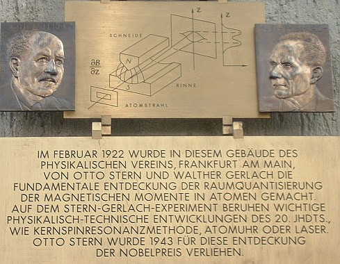
A plaque at Robert-Mayer Str. 2–4 in Frankfurt, Germany, commemorates the Stern-Gerlach experiment. (Courtesy: Horst Schmidt-Böcking)
One promising alternative is to, in effect, combine the Stern-Gerlach experiment with the electron double-slit experiment by using magnetic fields not only to separate out the distinct wave packets, but also to bring them back together and interfere them. The presence of interference fringes would then prove there is a definite phase relation between the two wave packets, which is the hallmark of pure quantum states – just as an interference pattern appears in the double-slit experiment even when electrons pass through the slits one at a time.
Building such an interferometer has long been considered extremely challenging, given that both the position and momentum of the separated wave packets need to be restored with very high accuracy for fringes to form. But recent advances in atom chips have changed the outlook. These tiny electric circuits trap atoms, ions or molecules just above their surface, and make it possible to produce strong magnetic field gradients much more accurately than is possible using macroscopic coils.
A full loop
Folman and colleagues released individual atoms of rubidium-87 from a magnetic trap beneath an atom chip and used a radio-frequency pulse to place them in a superposition of two spin states. By sending pulses of current through the chip, they then exposed the free-falling atoms to four magnetic gradients in quick succession – splitting each atom’s wave packets along two paths, halting the wave packets’ relative movement, bringing them back together and finally halting them again.
As Folman explains, the free-falling configuration ensured the cleanest possible environment for the experiment. “The four operations are very delicate as the final two are supposed to exactly undo the action of the first two,” he says. “And if you want to perfectly close the loop, you don’t want any other fields – from the trap – to get in your way.”
In a previous study, the researchers observed interference using a simpler set-up known as a half-loop Stern-Gerlach interferometer, in which they separated the wave packets and then allowed them to expand over time until they overlapped. In contrast, the new “full-loop” interferometer actively brings the wave packets back together, and detects interference through variations in spin population rather than a spatial fringe pattern. The researchers say that this more complex technique should make it possible to observe the interference more quickly, and without the need for high-resolution imaging.
Towards a super-sized superposition
In a paper published in Science Advances, Folman and colleagues (including theorists in Germany, the Netherlands and the UK) describe how the complete interferometer might be used to study the superposition of much larger objects. In particular, they lay out the challenges involved in interfering the wave packets of a nanoscale piece of diamond containing about a million carbon atoms and a single nitrogen-vacancy spin embedded within them.
One especially difficult aspect of this problem, they write, will be to recombine the wave packets in a spot smaller than the coherence length of the nano-diamond “particle”. Although new cooling techniques could up the nano-diamond’s coherence length to about 0.1 nm, the overlap accuracy of their experiment was only 100nm. Nevertheless, they are optimistic that they can improve the accuracy by the necessary three orders of magnitude by driving the atom chip with more precise current pulses.
If they can do that – while also minimizing environmental decoherence from scattered light, blackbody radiation or the magnetic fields – Folman says their device “could probe quantum mechanics and gravity in new regimes”. For example, detecting entanglement between two such devices placed side-by-side could put theories of quantum gravity to the test. Measuring gravitational interactions at short range might also make it possible to test for a putative fifth force. What’s more, they add, interferometers with large masses covering wide areas might be sensitive to new types of gravitational waves.
Gavin Morley of Warwick University in the UK, who was not involved with the latest research, is also upbeat. He argues that the new interferometer is “clearly ahead of competing technologies” when it comes to possible tests of quantum gravity. However, he cautions that the necessary enhancement of gravitational interactions and shielding of the nitrogen-vacancy spin will require nano particles with several billion, rather than million, atoms. “Smaller diamonds could test objective collapse theories and short-range gravity,” he adds.
This article was amended on 8 June 2021 to include photos of the atom chip used in the experiment and a plaque commemorating the work of Stern and Gerlach.
Ambient WiFi signals can be used to power small electrical devices such as LEDs, researchers in Singapore and Japan have shown. Hyunsoo Yang at the National University of Singapore and colleagues have developed a new way of connecting tiny microwave oscillators, allowing them to charge a capacitor that can then drive devices such as remote sensors. The research could also lead to the development of circuits that mimic the nervous system.
WiFi is ubiquitous in buildings and a growing number of public spaces, which are awash with 2.4 GHz microwaves used to exchange data. While this provides Internet access for the masses, large amounts of microwave energy goes to waste.
Yang’s team propose that this energy could be harvested to provide a wireless power source for small electrical devices, which would operate without any need for batteries. Their idea is based around emerging devices called spin-torque oscillators (STOs). These are nanoscale devices that can create and detect microwave signals and are compatible with commercial semiconductor manufacturing. Today, however, the usefulness of STOs is limited by their low power output and broadband nature.
Synchronized operation
These shortcomings can be overcome by synchronizing the outputs of multiple STOs. One way of doing this is to put the STOs microns apart, but this is unsuitable for efficient on-chip systems and does not work well for WiFi signals. Another possible solution is to couple the STOs using radio-frequency electrical signals, which is what Yang and colleagues have done.
When a configuration of eight STOs were connected in series, the team found that they could convert WiFi signals they received into a direct-current voltage that could charge a capacitor. They found that charging the capacitor for 5 s stored enough energy to power a 1.6-volt LED for 1 min.
The team also looked at how synchronization improved the STOs ability to broadcast gigahertz microwave signals and found that a parallel configuration is better suited for this application.
In future research, Yang’s team aim to upscale their energy harvesting techniques by increasing the numbers of STOs in their arrays, while also using them to charge other electrical devices and sensors. By working with industry partners, they hope to pave the way for every day, battery-free electronics, suitable for integration into networks of smart devices comprising the Internet of Things. Other possible applications for synchronized STOs include high-speed neuromorphic computing systems, which process information by mimicking biological nervous systems.
The chances are that when you watch a film, check your e-mail or surf the web, you’ll be staring at a screen populated with liquid crystals and backlit with LEDs. It’s a combination that has much merit: manufacturing costs are low, the picture is pretty good, and the display is relatively thin and lightweight – nothing like that associated with the cathode-ray tubes of yesteryear. But contrast ratios could be far higher, as could efficiencies, which would lengthen the battery life of portable devices.
Promising to address both these weaknesses is an emerging class of display that employs direct emission from red, green and blue LEDs. It is a technology that has existed for many years in magnified form, in the screens that adorn sporting stadia and a handful of prominent buildings in big cities. However, the construction of these large screens is time-consuming and costly, requiring millions of LEDs to be carefully positioned at precise locations. If this form of display is to be scaled down in size and up in volume, a new production approach will be needed to create screens based on direct-emitting microLEDs for TVs, laptops, smartphones and virtual-reality headsets.
A contender for this task is the massively parallel transfer printing technique pioneered by John Rodger’s team at the University of Illinois, Urbana-Champaign. This approach uses a stamp to pick up many microLEDs simultaneously from the wafer on which they were formed, and transfer them to a backplane, sometimes via an intermediary carrier. During this process, engineers can control the distance between each of the clusters of red, green and blue microLEDs that form a colour pixel. This degree of freedom is welcome when making large screens, such as those in supersize TVs, where it is folly to have colour pixels very close together – the benefits of such a high resolution would be wasted on the viewer, while the bill-of-materials would soar.
Right now, much effort within the nascent microLED display industry is directed at accelerating the throughput of this parallel transfer process. Today, a good ball-park for pick-and-place is 50,000 devices per hour. Cutting-edge developers, such as Samsung, may be faster. But given that an ultrahigh-definition display requires 25 million microLEDs, it takes many hours to construct a display via this approach.
Maybe, even with substantial improvement, it will never be possible to produce a mass-market display with a pick-and-place approach. That’s the view of Paul Schuele, CTO of US display developer eLux. “I just don’t believe it’s going to be economically feasible, apart from for show projects,” he argues.
Microfluidic mass transfer
Championing one of a handful of technologies to overcome this barrier, Schuele and co-workers have developed a microfluidic process with unprecedented throughput that’s capable of placing up to 50 million microLEDs per hour. Production begins by forming batches of a novel form of LED with a circular base and a post, before suspending them in their millions in solution. This suspension is cast over the surface of a display backplane populated with an array of circular holes, each located above an accompanying thin-film transistor. MicroLEDs that fall into the holes post-up are trapped, while those that enter post-down are unstable, soon to be dislodged by the forces of the fluid (figure 1). Once displaced, those microLEDs move on. It’s not long before they are permanently trapped post-up at another site, helping to fill up all the holes in the backplane. Electrical connections are then added to every microLED, using a low-temperature anneal to unite the solder on the backplane with that on a pair of contact rings on the device. Once this connection is in place, the thin-film transistor under every microLED controls its emission.
1 Go with the flow
(Courtesy: eLux)
eLux produces microLED displays by casting a solution of microLEDs over a backplane, where they are propelled by the moving fluid. If they enter a well post-up, they are trapped; if they enter post-down, fluid forces dislodge them.
This stochastic process for populating the holes cannot, on its own, produce a colour display. To form such a display, after filling holes with blue LEDs, the red and green components for every pixel are created by adding a colour-converting medium. Quantum dots are used for this task, rather than conventional phosphors, which Schuele describes as “big grains that are nasty to deal with”. While it is possible to reduce the size of the grains, this comes at the expense of efficiency.
To simplify their display architecture, Schuele and co-workers are developing a new process that avoids the use of quantum dots, by employing direct-emitting red, green and blue LEDs. One of the challenges with this is that the red LEDs, made on gallium-arsenide substrates, are not as amenable as their blue and green cousins, grown on sapphire, to the separation of the device from its substrate. While laser-lift off can extract blue and green emitters from sapphire, red microLEDs require etching to remove their substrate. This is not easy.
Another challenge facing the makers of high-quality displays comes from the incredible sensitivity of the eye to imperfections. Commercial success hinges on eradicating defects, which, for eLux, come in three forms: an absence of microLEDs, microLEDs that are plagued by a short, and those with insufficient brightness.
Colouring the pixels In an eLux microLED display, each cluster of six blue LEDs is transformed into a colour pixel by coating one pair with red-emitting quantum dots and another pair with green-emitting variants. (Courtesy: eLux)
Helping to address any absence of devices is a built-in redundancy, accomplished by using each transistor to drive two microLEDs in parallel. With this configuration, if one microLED is missing, it’s not an issue – there is a doubling of the current through the other microLED that masks the absence of its sibling. Unfortunately, this is not a fix for spots on the backplane where there are no microLEDs. “You can repair with pick-and-place, but my personal belief is that it is not economically viable,” says Schuele, who instead suggests a touch-up process, in which microLED solution is locally dispensed over the region with missing LEDs.
Schuele views shorts as a bigger issue, because they defeat redundancy. After identifying these renegades with thermal imaging, they can be repaired, but this is an expensive solution. So eLux prefers to identify the shorted LEDs on the device wafer and reject them.
To address the third issue – LEDs that are weak emitters – engineers screen device wafers and eliminate regions with insufficient efficiency. One powerful way to do this is to scan a focused laser beam across the wafer and record the intensity of the light emitted by the structure. Lower values expose weak LEDs.
Going forward, eLux may look to expand the range of sizes of its microLEDs. Today’s production process accommodates devices with diameters from about 150 μm to just 17 μm. Smaller sizes enable a higher pixel density and superior resolution. The current range is well suited to making TV displays, while the smaller sizes, which can easily realize a density of 300 pixels per inch, are also ideal for automotive and military displays where reliability and brightness are major assets. These microLEDs, however, are not nearly small enough for a virtual-reality headset.
The silicon solution
For that application, pixels must be no more than 5 μm in size and packed close together. It’s a pair of requirements fulfilled by another alternative to pick-and-place, being pursued by Plessey, a UK firm with a rich history in producing gallium nitride (GaN)-on-silicon LEDs.
Plessey’s production process begins by growing the layers of a GaN LED on a silicon wafer. This wafer is processed to define pixels separated by blocking material, which provides electrical and optical isolation. Bonding this processed wafer to a silicon backplane creates a display, before the growth substrate for the LEDs is removed to increase light extraction.
Using this approach, Plessey forms red, green and blue single-colour displays. Those emitting in the blue and green are made from direct-emitting LEDs – the green variant is less efficient, but this is offset by the eye’s superior sensitivity in this spectral domain – whilst that in the red uses blue LEDs to pump red-emitting quantum dots, due to difficulties in creating GaN LEDs that emit red light.
The other option for the red LED is the traditional phosphide-based emitter. But this would be incredibly challenging to produce on silicon. And, according to company CEO Keith Strickland, even if successful, such effort would offer dubious reward, due to the temperature instability of this form of LED. “I’ve seen degradation on phosphide materials of 40–50% as you go up a few tens of degrees or so,” he notes. In comparison, the decline in performance of GaN-based LEDs is around just 10%, leading to improved colour stability for the display.
Customers purchasing Plessey’s single-colour red, green and blue displays can form a full-colour display by combining their output with an X-prism. It’s an approach with pros and cons: it realizes a higher resolution compared with displays that have coloured pixels side by side; but it adds weight and bulkiness.
Underwater viewing After developing LEDs for horticultural lighting, towards the end of the last decade Plessey switched focus to microLEDs, cutting its teeth by developing display technology for a variety of assisted-reality products, including swimming googles that feature a stopwatch and a lap counter. (Courtesy: Plessey)
Plessey is working towards a single-wafer solution, which requires red, green and blue LEDs to be grown in a single stack. That’s not easy, as different temperatures are needed for different emission wavelengths, and higher temperatures threaten to wreak havoc on deposited structures. However, progress has been made, with blue and green pixels produced on the same wafer. The company has also made strides at longer wavelengths, realizing a red-emitting GaN-based LED, a notoriously challenging device to produce.
To gain traction in the display industry, Plessey began by marketing its technology for assisted-reality displays, such as scuba-diving masks incorporating a dive computer, swimming googles with a lap clock and gun-scopes featuring a range finder. The publicity generated by this raised the company’s profile, and may well have played a key role in helping it to clinch a deal with Facebook, signed last March. Plessey’s technology is seen as a great fit for Facebook’s augmented-reality and virtual-reality products, such as its Oculus Quest headsets.
With such big names investing in microLED displays, the future is very bright for this technology. The approaches of eLux and Plessey clearly have much promise, giving them a great chance of competing against pick-and-place technologies and other rival approaches in a growing market that could be worth billions of dollars by the middle of this decade.